
Lattice Semiconductor Corporation
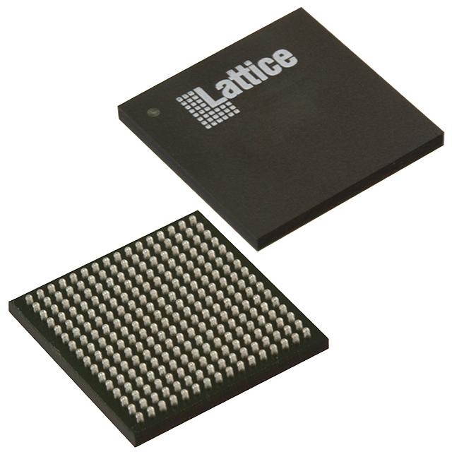
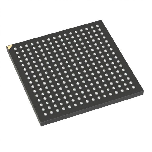
LCMXO1200E-5B256C
LCMXO1200E-5B256C ECAD Model
LCMXO1200E-5B256C Attributes
| Type | Description | Select |
|---|---|---|
| Mfr | Lattice Semiconductor Corporation | |
| Series | MachXO | |
| Package | Tray | |
| Number of LABs/CLBs | 150 | |
| Number of Logic Elements/Cells | 1200 | |
| Total RAM Bits | 9421 | |
| Number of I/O | 211 | |
| Voltage - Supply | 1.14V ~ 1.26V | |
| Mounting Type | Surface Mount | |
| Operating Temperature | 0°C ~ 85°C (TJ) | |
| Package / Case | 256-LFBGA, CSPBGA | |
| Supplier Device Package | 256-CABGA (14x14) | |
| Base Product Number | LCMXO1200 |
LCMXO1200E-5B256C Datasheet Download
LCMXO1200E-5B256C Overview
The LCMXO1200E-5B256C is a Field Programmable Gate Array (FPGA) chip from Lattice Semiconductor. It is a low-cost, low-power, small-footprint device that can be used for a variety of applications.
The LCMXO1200E-5B256C is built using the Lattice CrossLink-NX FPGA architecture, which is optimized for low-cost, low-power, and small-footprint applications. It has a total of 256 logic cells and up to 5.7Kbits of block RAM. It also has up to 4 DSP blocks, 4 I/O Banks, and a wide range of I/O options. The chip is also equipped with a variety of features such as clock management, JTAG, and flash memory support.
The LCMXO1200E-5B256C has a wide variety of applications and can be used for a variety of purposes. It can be used for embedded systems, industrial automation, consumer products, automotive, medical, and other applications. It can also be used for communication systems such as Ethernet, USB, and CAN.
Overall, the LCMXO1200E-5B256C is an ideal choice for low-cost, low-power, and small-footprint applications. It is a highly versatile chip that can be used for a variety of applications. Its wide range of features and I/O options make it an ideal choice for a variety of projects.
You May Also Be Interested In
2,228 In Stock
Pricing (USD)
| QTY | Unit Price | Ext Price |
|---|---|---|
| No reference price found. | ||