
Lattice Semiconductor Corporation
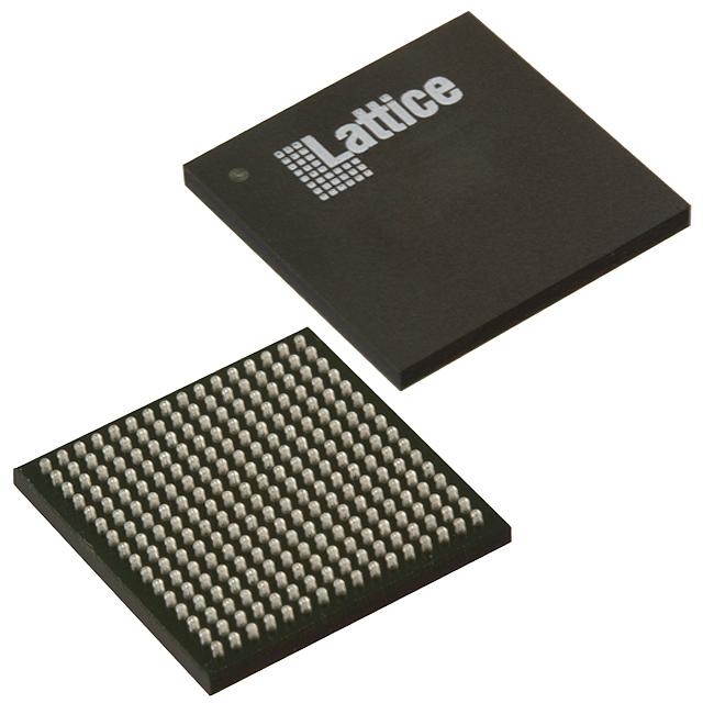
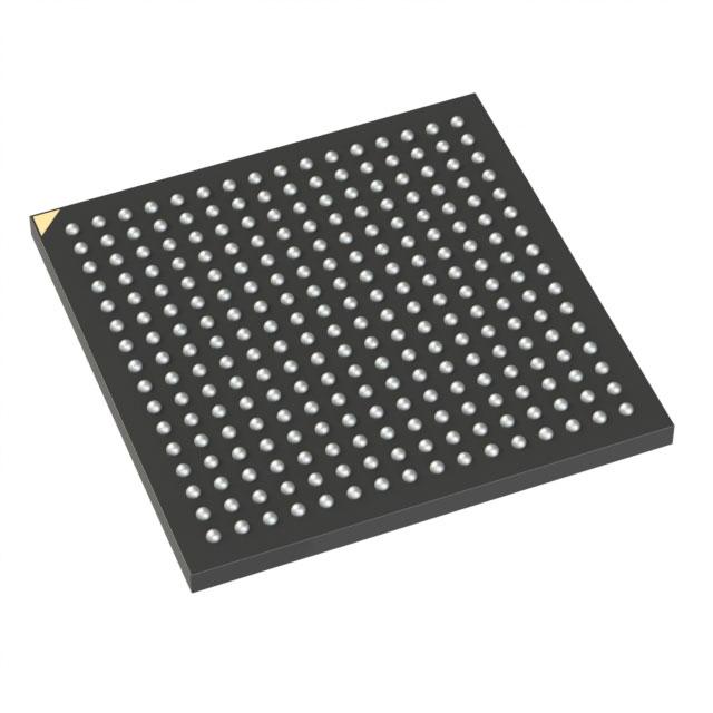
LCMXO1200E-4B256I
LCMXO1200E-4B256I ECAD Model
LCMXO1200E-4B256I Attributes
| Type | Description | Select |
|---|---|---|
| Mfr | Lattice Semiconductor Corporation | |
| Series | MachXO | |
| Package | Tray | |
| Number of LABs/CLBs | 150 | |
| Number of Logic Elements/Cells | 1200 | |
| Total RAM Bits | 9421 | |
| Number of I/O | 211 | |
| Voltage - Supply | 1.14V ~ 1.26V | |
| Mounting Type | Surface Mount | |
| Operating Temperature | -40°C ~ 100°C (TJ) | |
| Package / Case | 256-LFBGA, CSPBGA | |
| Supplier Device Package | 256-CABGA (14x14) | |
| Base Product Number | LCMXO1200 |
LCMXO1200E-4B256I Datasheet Download
LCMXO1200E-4B256I Overview
The LCMXO1200E-4B256I is a low-cost, low-power, field-programmable gate array (FPGA) chip model designed by Lattice Semiconductor. It is a member of the Lattice CrossLink family of FPGAs and is targeted at applications requiring high speed and low power consumption.
The LCMXO1200E-4B256I FPGA chip model is based on the Lattice CrossLink architecture and is manufactured using a 0.35µm CMOS process. It offers 256Kbits of internal RAM and has a maximum operating frequency of up to 250 MHz. It has a total of four I/O banks, each with up to 32 I/Os. It also features a wide range of features such as clock synchronization, clock gating, and programmable I/O voltage.
The LCMXO1200E-4B256I is suitable for a wide range of applications, such as industrial automation, medical devices, consumer electronics, automotive, and aerospace. It can be used in applications requiring low power consumption, high speed, and low cost. It is also suitable for applications requiring high data rates, such as video and image processing, communications, and networking.
The LCMXO1200E-4B256I is available in a range of packages, including TQFP, VFBGA, and TFBGA. It is also RoHS compliant, making it an ideal choice for a wide range of applications.
You May Also Be Interested In
2,803 In Stock
Pricing (USD)
| QTY | Unit Price | Ext Price |
|---|---|---|
| No reference price found. | ||