

Lattice Semiconductor Corporation
LC4256V-75TN176E
LC4256V-75TN176E ECAD Model
LC4256V-75TN176E Attributes
| Type | Description | Select |
|---|---|---|
| Mfr | Lattice Semiconductor Corporation | |
| Series | ispMACH® 4000V | |
| Package | Tray | |
| Programmable Type | In System Programmable | |
| Delay Time tpd(1) Max | 7.5 ns | |
| Voltage Supply - Internal | 3V ~ 3.6V | |
| Number of Logic Elements/Blocks | 16 | |
| Number of Macrocells | 256 | |
| Number of I/O | 128 | |
| Operating Temperature | -40°C ~ 130°C (TJ) | |
| Mounting Type | Surface Mount | |
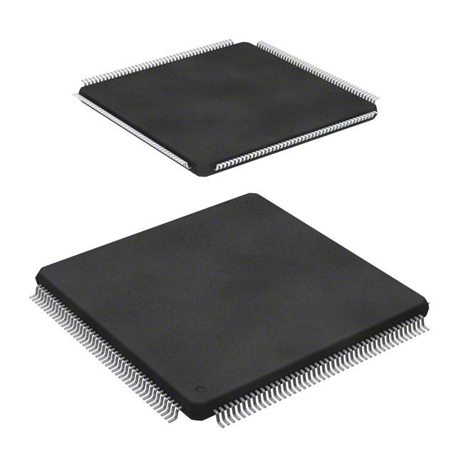
| Package / Case | 176-LQFP | |
| Supplier Device Package | 176-TQFP (24x24) | |
| Base Product Number | LC4256 |
LC4256V-75TN176E Datasheet Download
LC4256V-75TN176E Overview
The chip model LC4256V-75TN176E is a product manufactured by Lattice Semiconductor Corporation. It is a low-cost, low-power, highly-flexible, and high-density Field Programmable Gate Array (FPGA). The chip model LC4256V-75TN176E is designed to meet the needs of advanced communication systems, such as 5G and beyond. This chip model has been designed with a wide range of features, including an on-chip memory of 256 Kbits, an on-chip DSP block, and a wide range of I/O options.
The original design intention of the LC4256V-75TN176E was to provide a cost-effective and flexible solution for advanced communication systems. The chip model is designed to be easily upgradable and can be used in a wide range of applications. It is also possible to integrate the chip model into existing systems, allowing for a seamless transition.
The LC4256V-75TN176E can be used in a variety of advanced communication systems, such as 5G and beyond. It is also suitable for use in the era of fully intelligent systems, such as the Internet of Things (IoT), autonomous vehicles, and smart cities. The chip model can be used in a variety of intelligent scenarios, such as facial recognition, natural language processing, and machine learning.
The product description and specific design requirements of the chip model LC4256V-75TN176E are detailed in the product data sheet. The chip model is designed to meet the needs of advanced communication systems, with features such as an on-chip memory of 256 Kbits, an on-chip DSP block, and a wide range of I/O options. The chip model is also designed to be easily upgradable and can be used in a wide range of applications.
In addition to the product description and design requirements, there are also case studies and precautions to consider when using the chip model LC4256V-75TN176E. For example, the chip model may require additional components and/or external circuitry in order to function properly. Furthermore, the chip model may not be suitable for certain applications due to its limited memory and processing capabilities. It is therefore important to consider the specific requirements of the application before using the chip model.
In conclusion, the chip model LC4256V-75TN176E is a low-cost, low-power, highly-flexible, and high-density Field Programmable Gate Array (FPGA). It is designed to meet the needs of advanced communication systems, such as 5G and beyond. The chip model can be used in a variety of intelligent scenarios, such as facial recognition, natural language processing, and machine learning. The product description and design requirements of the chip model are detailed in the product data sheet, and case studies and precautions should be considered when using the chip model.
You May Also Be Interested In
5,325 In Stock
Pricing (USD)
| QTY | Unit Price | Ext Price |
|---|---|---|
| 1+ | $54.0310 | $54.0310 |
| 10+ | $53.4500 | $534.4998 |
| 100+ | $50.5451 | $5,054.5086 |
| 1000+ | $47.6402 | $23,820.0980 |
| 10000+ | $43.5734 | $43,573.3500 |
| The price is for reference only, please refer to the actual quotation! | ||