
AMD Xilinx
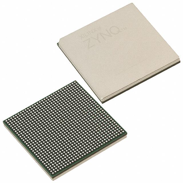
XCZU5CG-L2FBVB900E
XCZU5CG-L2FBVB900E ECAD Model
XCZU5CG-L2FBVB900E Attributes
| Type | Description | Select |
|---|---|---|
| Rohs Code | Yes | |
| Part Life Cycle Code | Active | |
| Surface Mount | YES | |
| Supply Voltage-Nom | 720 mV | |
| uPs/uCs/Peripheral ICs Type | MICROPROCESSOR CIRCUIT | |
| Technology | CMOS | |
| Additional Feature | ALSO AVAILABLE WITH 0.85V NOMINAL SUPPLY | |
| Supply Voltage-Max | 742 mV | |
| Supply Voltage-Min | 698 mV | |
| Temperature Grade | OTHER | |
| JESD-30 Code | R-PBGA-B900 | |
| JESD-609 Code | e1 | |
| Moisture Sensitivity Level | 4 | |
| Operating Temperature-Max | 110 °C | |
| Peak Reflow Temperature (Cel) | 245 | |
| Time@Peak Reflow Temperature-Max (s) | 30 | |
| Number of Terminals | 900 | |
| Package Body Material | PLASTIC/EPOXY | |
| Package Code | BGA | |
| Package Shape | RECTANGULAR | |
| Package Style | GRID ARRAY | |
| Terminal Finish | Tin/Silver/Copper (Sn96.5Ag3.0Cu0.5) | |
| Terminal Form | BALL | |
| Terminal Position | BOTTOM | |
| Ihs Manufacturer | XILINX INC | |
| Package Description | BGA, BGA900,30X30,40 | |
| Reach Compliance Code | compliant | |
| ECCN Code | 5A002.A.4 | |
| HTS Code | 8542.39.00.01 |
XCZU5CG-L2FBVB900E Datasheet Download
XCZU5CG-L2FBVB900E Overview
The chip model XCZU5CG-L2FBVB900E is a high-performance, low-power FPGA designed for applications in the defense, aerospace, medical, industrial, and communication industries. Manufactured by Xilinx, the chip model is part of the UltraScale+ family of FPGAs and is designed to deliver the highest levels of performance, system integration, and scalability.
The XCZU5CG-L2FBVB900E is well suited for applications that require high-speed, low-power, and reliable operation. It features a high-speed transceiver with up to 28.1 Gbps data rate, a low-power embedded processor, and a high-performance memory interface. The chip model also offers a wide range of features, such as advanced power management, multi-rail power, and programmable logic blocks.
The XCZU5CG-L2FBVB900E is expected to be in high demand in the future, particularly in the defense and aerospace industries. The chip model is designed to support advanced communication systems, such as 5G and beyond, and is capable of providing high-speed data transmission with low latency. Additionally, the chip model can be upgraded to support new technologies, such as artificial intelligence and machine learning, in the future.
The original design intention of the XCZU5CG-L2FBVB900E was to provide a high-performance, low-power FPGA for applications in the defense, aerospace, medical, industrial, and communication industries. The chip model is designed to be flexible and scalable, offering a wide range of features and allowing for future upgrades. This makes it an ideal choice for applications that require the highest levels of performance, system integration, and scalability.
The XCZU5CG-L2FBVB900E is expected to be in high demand in the future, particularly in the defense and aerospace industries. The chip model is capable of supporting advanced communication systems, such as 5G and beyond, and is also capable of being upgraded to support new technologies, such as artificial intelligence and machine learning. As a result, the chip model is well suited for applications that require high-speed, low-power, and reliable operation.
You May Also Be Interested In

5,508 In Stock
Pricing (USD)
| QTY | Unit Price | Ext Price |
|---|---|---|
| 1+ | $1,891.5530 | $1,891.5530 |
| 10+ | $1,871.2138 | $18,712.1376 |
| 100+ | $1,769.5174 | $176,951.7360 |
| 1000+ | $1,667.8210 | $833,910.4800 |
| 10000+ | $1,525.4460 | $1,525,446.0000 |
| The price is for reference only, please refer to the actual quotation! | ||