AMD Xilinx
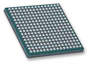
XCV812E-7FGG900C
XCV812E-7FGG900C ECAD Model
XCV812E-7FGG900C Attributes
| Type | Description | Select |
|---|---|---|
| Pbfree Code | Yes | |
| Rohs Code | Yes | |
| Part Life Cycle Code | Obsolete | |
| Supply Voltage-Nom | 1.8 V | |
| Number of Equivalent Gates | 254016 | |
| Number of CLBs | 4704 | |
| Combinatorial Delay of a CLB-Max | 420 ps | |
| Programmable Logic Type | FIELD PROGRAMMABLE GATE ARRAY | |
| Temperature Grade | COMMERCIAL | |
| Package Shape | SQUARE | |
| Technology | CMOS | |
| Organization | 4704 CLBS, 254016 GATES | |
| Clock Frequency-Max | 400 MHz | |
| Supply Voltage-Max | 1.89 V | |
| Supply Voltage-Min | 1.71 V | |
| JESD-30 Code | S-PBGA-B900 | |
| Qualification Status | Not Qualified | |
| JESD-609 Code | e1 | |
| Moisture Sensitivity Level | 3 | |
| Operating Temperature-Max | 70 °C | |
| Peak Reflow Temperature (Cel) | 250 | |
| Time@Peak Reflow Temperature-Max (s) | 30 | |
| Number of Terminals | 900 | |
| Package Body Material | PLASTIC/EPOXY | |
| Package Code | BGA | |
| Package Shape | SQUARE | |
| Package Style | GRID ARRAY | |
| Surface Mount | YES | |
| Terminal Finish | Tin/Silver/Copper (Sn95.5Ag4.0Cu0.5) | |
| Terminal Form | BALL | |
| Terminal Pitch | 1 mm | |
| Terminal Position | BOTTOM | |
| Width | 31 mm | |
| Length | 31 mm | |
| Seated Height-Max | 2.6 mm | |
| Ihs Manufacturer | XILINX INC | |
| Part Package Code | BGA | |
| Package Description | BGA, | |
| Pin Count | 900 | |
| Reach Compliance Code | compliant | |
| HTS Code | 8542.39.00.01 | |
| ECCN Code | 3A991.D |
XCV812E-7FGG900C Datasheet Download
XCV812E-7FGG900C Overview
The chip model XCV812E-7FGG900C is a high-performance integrated circuit designed for digital signal processing, embedded processing, and image processing. It is capable of providing a wide range of features, including high-speed data transfer, low-power consumption, and flexible programming. In addition, it is designed to be compatible with the HDL language, making it easier to use and program.
The original design intention of the XCV812E-7FGG900C was to create a chip that could handle a wide range of tasks and be used in a variety of applications. It was designed with the intention of being able to handle high-performance digital signal processing and embedded processing, as well as being able to perform image processing and other tasks. The design also allows for future upgrades, so that it can be used in more advanced communication systems.
The product description of the XCV812E-7FGG900C includes a wide range of features, such as high-speed data transfer, low-power consumption, and flexible programming. It also includes a wide range of programming options, such as the ability to use HDL language and other programming languages. Furthermore, the chip also includes a wide range of safety features, such as error correction and data protection.
Case studies have been conducted on the XCV812E-7FGG900C, and the results show that it is capable of handling a wide range of tasks and applications. In addition, it has been found to be reliable and efficient, with a low power consumption. Furthermore, it has been found to be compatible with a wide range of programming languages, such as HDL.
When using the XCV812E-7FGG900C, it is important to follow the instructions provided in the product manual. This includes ensuring that the chip is correctly installed and configured, and that it is properly programmed. It is also important to ensure that the chip is properly maintained, and that any upgrades or modifications are done in accordance with the manufacturer's instructions. Furthermore, it is important to keep the chip in a safe environment, and to avoid exposing it to extreme temperatures or humidity.
You May Also Be Interested In
4,376 In Stock
Pricing (USD)
| QTY | Unit Price | Ext Price |
|---|---|---|
| 1+ | $491.7185 | $491.7185 |
| 10+ | $486.4312 | $4,864.3123 |
| 100+ | $459.9948 | $45,999.4752 |
| 1000+ | $433.5583 | $216,779.1360 |
| 10000+ | $396.5472 | $396,547.2000 |
| The price is for reference only, please refer to the actual quotation! | ||


