
AMD Xilinx
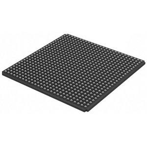
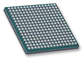
XCV800-6FGG676I
XCV800-6FGG676I ECAD Model
XCV800-6FGG676I Attributes
| Type | Description | Select |
|---|---|---|
| Pbfree Code | Yes | |
| Rohs Code | Yes | |
| Part Life Cycle Code | Obsolete | |
| Supply Voltage-Nom | 2.5 V | |
| Number of Equivalent Gates | 888439 | |
| Number of CLBs | 4704 | |
| Combinatorial Delay of a CLB-Max | 600 ps | |
| Programmable Logic Type | FIELD PROGRAMMABLE GATE ARRAY | |
| Package Shape | SQUARE | |
| Technology | CMOS | |
| Organization | 4704 CLBS, 888439 GATES | |
| Clock Frequency-Max | 333 MHz | |
| Supply Voltage-Max | 2.625 V | |
| Supply Voltage-Min | 2.375 V | |
| JESD-30 Code | S-PBGA-B676 | |
| Qualification Status | Not Qualified | |
| JESD-609 Code | e1 | |
| Moisture Sensitivity Level | 3 | |
| Peak Reflow Temperature (Cel) | 250 | |
| Time@Peak Reflow Temperature-Max (s) | 30 | |
| Number of Terminals | 676 | |
| Package Body Material | PLASTIC/EPOXY | |
| Package Code | BGA | |
| Package Shape | SQUARE | |
| Package Style | GRID ARRAY | |
| Surface Mount | YES | |
| Terminal Finish | Tin/Silver/Copper (Sn95.5Ag4.0Cu0.5) | |
| Terminal Form | BALL | |
| Terminal Pitch | 1 mm | |
| Terminal Position | BOTTOM | |
| Width | 27 mm | |
| Length | 27 mm | |
| Seated Height-Max | 2.6 mm | |
| Ihs Manufacturer | XILINX INC | |
| Part Package Code | BGA | |
| Package Description | BGA, | |
| Pin Count | 676 | |
| Reach Compliance Code | compliant | |
| HTS Code | 8542.39.00.01 |
XCV800-6FGG676I Datasheet Download
XCV800-6FGG676I Overview
The chip model XCV800-6FGG676I is a high-performance integrated circuit that is suitable for various digital signal processing applications, such as embedded processing, image processing, and so on. It requires the use of HDL language to program and operate. This chip model is an advanced solution for high-performance digital signal processing, and has been widely adopted by various industries.
The industry trends of the chip model XCV800-6FGG676I and the future development of related industries depend on what specific technologies are needed. It is important to note that the application environment may require the support of new technologies in order to keep up with the development of the industry.
The original design intention of the chip model XCV800-6FGG676I is to provide a powerful solution for digital signal processing applications. The chip is designed with a high level of efficiency and performance in mind, and is capable of being upgraded in the future to meet the needs of more advanced applications. In addition, the chip model is also suitable for advanced communication systems, such as 5G and beyond.
To conclude, the chip model XCV800-6FGG676I is a powerful solution for digital signal processing applications, and is capable of being upgraded in the future to meet the needs of more advanced applications. It is suitable for various applications, such as embedded processing, image processing, and advanced communication systems. The application environment may require the support of new technologies in order to keep up with the development of the industry.
You May Also Be Interested In

1,539 In Stock
Pricing (USD)
| QTY | Unit Price | Ext Price |
|---|---|---|
| No reference price found. | ||