
AMD Xilinx
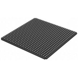
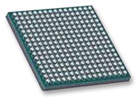
XCV400-6FGG676I
XCV400-6FGG676I ECAD Model
XCV400-6FGG676I Attributes
| Type | Description | Select |
|---|---|---|
| Pbfree Code | Yes | |
| Rohs Code | Yes | |
| Part Life Cycle Code | Obsolete | |
| Supply Voltage-Nom | 2.5 V | |
| Number of Equivalent Gates | 468252 | |
| Number of CLBs | 2400 | |
| Combinatorial Delay of a CLB-Max | 600 ps | |
| Programmable Logic Type | FIELD PROGRAMMABLE GATE ARRAY | |
| Package Shape | SQUARE | |
| Technology | CMOS | |
| Organization | 2400 CLBS, 468252 GATES | |
| Clock Frequency-Max | 333 MHz | |
| Supply Voltage-Max | 2.625 V | |
| Supply Voltage-Min | 2.375 V | |
| JESD-30 Code | S-PBGA-B676 | |
| Qualification Status | Not Qualified | |
| JESD-609 Code | e1 | |
| Moisture Sensitivity Level | 3 | |
| Peak Reflow Temperature (Cel) | 250 | |
| Time@Peak Reflow Temperature-Max (s) | 30 | |
| Number of Terminals | 676 | |
| Package Body Material | PLASTIC/EPOXY | |
| Package Code | BGA | |
| Package Shape | SQUARE | |
| Package Style | GRID ARRAY | |
| Surface Mount | YES | |
| Terminal Finish | Tin/Silver/Copper (Sn95.5Ag4.0Cu0.5) | |
| Terminal Form | BALL | |
| Terminal Pitch | 1 mm | |
| Terminal Position | BOTTOM | |
| Width | 27 mm | |
| Length | 27 mm | |
| Seated Height-Max | 2.6 mm | |
| Ihs Manufacturer | XILINX INC | |
| Part Package Code | BGA | |
| Package Description | BGA, | |
| Pin Count | 676 | |
| Reach Compliance Code | compliant | |
| HTS Code | 8542.39.00.01 |
XCV400-6FGG676I Datasheet Download
XCV400-6FGG676I Overview
The XCV400-6FGG676I chip model is a powerful tool for digital signal processing, embedded processing, and image processing. It is designed to be used with the HDL language, allowing for a more efficient and accurate development process. With its high-performance capabilities, the XCV400-6FGG676I chip model is suitable for a variety of applications, including but not limited to, digital signal processing, embedded processing, and image processing.
The XCV400-6FGG676I chip model is an ideal choice for those who need a reliable and powerful tool for their digital signal processing, embedded processing, and image processing needs. It is designed to be used with the HDL language, providing a more efficient and accurate development process. The chip model is designed to be flexible, offering a variety of features that can be tailored to meet the needs of different applications.
The XCV400-6FGG676I chip model is well suited for the demands of the future. With its high-performance capabilities, the chip model is expected to be in high demand in the coming years. This is due to the increasing demand for digital signal processing, embedded processing, and image processing applications. As new technologies emerge, the chip model will be able to meet the needs of these new technologies.
The XCV400-6FGG676I chip model offers a number of advantages. It is designed to be efficient and accurate, providing a reliable and powerful tool for digital signal processing, embedded processing, and image processing needs. It is also designed to be flexible, allowing for a variety of features that can be tailored to meet the needs of different applications.
In conclusion, the XCV400-6FGG676I chip model is an ideal choice for those who need a reliable and powerful tool for their digital signal processing, embedded processing, and image processing needs. With its high-performance capabilities, the chip model is expected to be in high demand in the coming years. As new technologies emerge, the chip model will be able to meet the needs of these new technologies, making it an ideal choice for those who need a reliable and powerful tool for their digital signal processing, embedded processing, and image processing needs.
You May Also Be Interested In

2,775 In Stock
Pricing (USD)
| QTY | Unit Price | Ext Price |
|---|---|---|
| 1+ | $178.5600 | $178.5600 |
| 10+ | $176.6400 | $1,766.4000 |
| 100+ | $167.0400 | $16,704.0000 |
| 1000+ | $157.4400 | $78,720.0000 |
| 10000+ | $144.0000 | $144,000.0000 |
| The price is for reference only, please refer to the actual quotation! | ||