AMD Xilinx
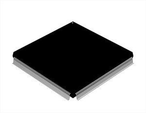
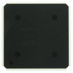
XCV100-5PQG240I
XCV100-5PQG240I ECAD Model
XCV100-5PQG240I Attributes
| Type | Description | Select |
|---|---|---|
| Rohs Code | Yes | |
| Part Life Cycle Code | Obsolete | |
| Supply Voltage-Nom | 2.5 V | |
| Number of Equivalent Gates | 108904 | |
| Number of CLBs | 600 | |
| Combinatorial Delay of a CLB-Max | 700 ps | |
| Programmable Logic Type | FIELD PROGRAMMABLE GATE ARRAY | |
| Package Shape | SQUARE | |
| Technology | CMOS | |
| Organization | 600 CLBS, 108904 GATES | |
| Clock Frequency-Max | 294 MHz | |
| Supply Voltage-Max | 2.625 V | |
| Supply Voltage-Min | 2.375 V | |
| JESD-30 Code | S-PQFP-G240 | |
| Qualification Status | Not Qualified | |
| JESD-609 Code | e3 | |
| Moisture Sensitivity Level | 3 | |
| Peak Reflow Temperature (Cel) | 245 | |
| Time@Peak Reflow Temperature-Max (s) | 30 | |
| Number of Terminals | 240 | |
| Package Body Material | PLASTIC/EPOXY | |
| Package Code | FQFP | |
| Package Shape | SQUARE | |
| Package Style | FLATPACK, FINE PITCH | |
| Surface Mount | YES | |
| Terminal Finish | Matte Tin (Sn) | |
| Terminal Form | GULL WING | |
| Terminal Pitch | 500 µm | |
| Terminal Position | QUAD | |
| Width | 32 mm | |
| Length | 32 mm | |
| Seated Height-Max | 4.1 mm | |
| Ihs Manufacturer | XILINX INC | |
| Part Package Code | QFP | |
| Package Description | FQFP, | |
| Pin Count | 240 | |
| Reach Compliance Code | compliant | |
| HTS Code | 8542.39.00.01 |
XCV100-5PQG240I Datasheet Download
XCV100-5PQG240I Overview
The XCV100-5PQG240I is a state-of-the-art chip model that offers powerful performance for high-performance digital signal processing, embedded processing, and image processing. It is designed to be used with HDL language, allowing for the creation of complex, yet efficient designs. The chip model is also capable of future upgrades, making it a suitable choice for advanced communication systems.
The XCV100-5PQG240I is a high-performance programmable logic device, featuring a 5-stage pipeline, a fast clock speed, and a low power consumption rate. It is designed to provide a wide range of features, such as support for multiple clock domains, high-speed I/O interfaces, and a wide variety of memory options. Additionally, it features a reconfigurable architecture, allowing for the design of complex, yet efficient designs.
The product description of the XCV100-5PQG240I includes a wide range of features and capabilities. It is designed to offer a high-performance, low-power solution for digital signal processing, embedded processing, and image processing. Furthermore, the chip model is capable of supporting multiple clock domains, high-speed I/O interfaces, and a wide variety of memory options. Additionally, the chip model is designed to be used with HDL language, allowing for the creation of complex, yet efficient designs.
When using the XCV100-5PQG240I, it is important to consider the design requirements and actual case studies. The design requirements should include the clock speed, memory options, I/O interfaces, and the HDL language. Additionally, it is important to consider the actual case studies, such as the performance and power consumption rate. Furthermore, it is important to consider the design trade-offs and the possibility of future upgrades.
In conclusion, the XCV100-5PQG240I is a powerful chip model that offers high-performance digital signal processing, embedded processing, and image processing. It is designed to be used with HDL language, allowing for the creation of complex, yet efficient designs. Furthermore, the chip model is capable of future upgrades, making it a suitable choice for advanced communication systems. When using the XCV100-5PQG240I, it is important to consider the design requirements and actual case studies, as well as the design trade-offs and the possibility of future upgrades.
You May Also Be Interested In
5,767 In Stock
Pricing (USD)
| QTY | Unit Price | Ext Price |
|---|---|---|
| No reference price found. | ||

