
AMD Xilinx
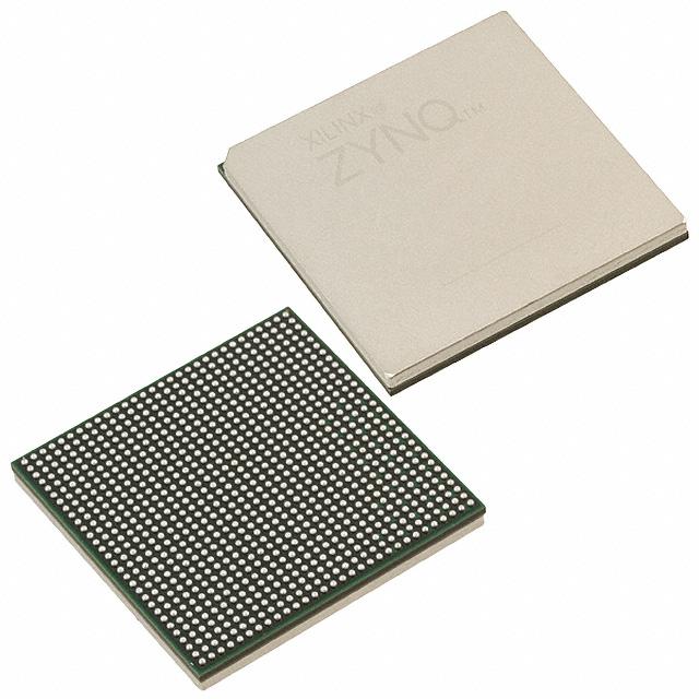
XC7Z045-1FFG900I
XC7Z045-1FFG900I ECAD Model
XC7Z045-1FFG900I Attributes
| Type | Description | Select |
|---|---|---|
| Rohs Code | Yes | |
| Part Life Cycle Code | Active | |
| Surface Mount | YES | |
| Supply Voltage-Nom | 1 V | |
| uPs/uCs/Peripheral ICs Type | SYSTEM ON CHIP | |
| Technology | CMOS | |
| Supply Voltage-Max | 1.05 V | |
| Supply Voltage-Min | 950 mV | |
| JESD-30 Code | S-PBGA-B900 | |
| Operating Temperature-Max | 100 °C | |
| Operating Temperature-Min | -40 °C | |
| Number of Terminals | 900 | |
| Package Body Material | PLASTIC/EPOXY | |
| Package Code | BGA | |
| Package Equivalence Code | BGA900,30X30,40 | |
| Package Shape | SQUARE | |
| Package Style | GRID ARRAY | |
| Terminal Form | BALL | |
| Terminal Pitch | 1 mm | |
| Terminal Position | BOTTOM | |
| Seated Height-Max | 3.24 mm | |
| Width | 27 mm | |
| Length | 27 mm | |
| Ihs Manufacturer | XILINX INC | |
| Package Description | FBGA-900 | |
| Reach Compliance Code | not_compliant | |
| ECCN Code | 3A991.D | |
| HTS Code | 8542.39.00.01 |
XC7Z045-1FFG900I Datasheet Download
XC7Z045-1FFG900I Overview
The Xilinx XC7Z045-1FFG900I is a field programmable gate array (FPGA) chip designed to meet the needs of a wide range of applications. This chip is capable of supporting a variety of technologies, including high-speed serial transceivers, DDR3 SDRAM, QSPI Flash, and Gigabit Ethernet. It is a powerful chip with a wide range of capabilities and features, making it a great choice for many applications.
The XC7Z045-1FFG900I is designed for high-performance applications, and its features make it a great choice for a variety of applications. It is capable of supporting up to 4.5 Gbps transceiver speeds and is designed to meet the needs of advanced communication systems. It also offers DDR3 SDRAM support, allowing for high-speed data transfer and storage. Additionally, it has on-chip QSPI Flash memory and Gigabit Ethernet support, making it a great choice for applications that require high-speed data transfer and storage.
The XC7Z045-1FFG900I also has a variety of design features that make it a great choice for a wide range of applications. It has a wide range of I/O capabilities, including dedicated transceiver channels and high-speed LVDS I/O. It also has a variety of on-chip features, such as built-in clock management, power management, and a wide range of on-chip debugging tools. Additionally, it is designed to be upgradeable, allowing for future upgrades and enhancements.
The XC7Z045-1FFG900I is a powerful chip that is capable of meeting the needs of a wide range of applications. It is designed for high-performance applications and has a wide range of features and capabilities. It is also upgradeable and can be used in advanced communication systems. In addition, it is designed with a variety of on-chip features, such as clock management and power management, making it a great choice for applications that require high-speed data transfer and storage.
When considering the use of the XC7Z045-1FFG900I, it is important to understand the product description and specific design requirements. Additionally, actual case studies and precautions should be taken into consideration. This will ensure that the chip is used in the most optimal way, and that any potential issues are addressed before they become a problem. It is also important to understand the industry trends and future development of related industries, as well as whether the application environment requires the support of new technologies. By understanding the original design intention of the chip and the possibility of future upgrades, it is possible to make an informed decision about the use of this chip.
You May Also Be Interested In

3,138 In Stock
Pricing (USD)
| QTY | Unit Price | Ext Price |
|---|---|---|
| 1+ | $6,875.8135 | $6,875.8135 |
| 10+ | $6,801.8801 | $68,018.8007 |
| 100+ | $6,432.2127 | $643,221.2673 |
| 1000+ | $6,062.5453 | $3,031,272.6390 |
| 10000+ | $5,545.0109 | $5,545,010.9250 |
| The price is for reference only, please refer to the actual quotation! | ||