
AMD Xilinx
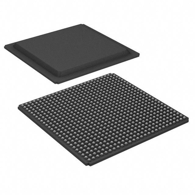
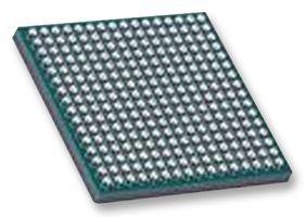
XC7Z035-L2FFG676I
XC7Z035-L2FFG676I ECAD Model
XC7Z035-L2FFG676I Attributes
| Type | Description | Select |
|---|---|---|
| Rohs Code | Yes | |
| Part Life Cycle Code | Active | |
| Surface Mount | YES | |
| Supply Voltage-Nom | 1 V | |
| uPs/uCs/Peripheral ICs Type | SYSTEM ON CHIP | |
| Technology | CMOS | |
| Supply Voltage-Max | 1.05 V | |
| Supply Voltage-Min | 950 mV | |
| JESD-30 Code | S-PBGA-B676 | |
| Operating Temperature-Max | 100 °C | |
| Operating Temperature-Min | -40 °C | |
| Number of Terminals | 676 | |
| Package Body Material | PLASTIC/EPOXY | |
| Package Code | BGA | |
| Package Equivalence Code | BGA676,26X26,40 | |
| Package Shape | SQUARE | |
| Package Style | GRID ARRAY | |
| Terminal Form | BALL | |
| Terminal Pitch | 1 mm | |
| Terminal Position | BOTTOM | |
| Seated Height-Max | 3.24 mm | |
| Width | 27 mm | |
| Length | 27 mm | |
| Ihs Manufacturer | XILINX INC | |
| Package Description | BGA, | |
| Reach Compliance Code | compliant | |
| ECCN Code | 3A991.D | |
| HTS Code | 8542.39.00.01 |
XC7Z035-L2FFG676I Datasheet Download
XC7Z035-L2FFG676I Overview
The XC7Z035-L2FFG676I chip model is a high-performance, low-power FPGA that has been designed with a wide range of applications in mind. It is suitable for use in advanced communication systems and can be used to develop and popularize future intelligent robots.
The original design intention of the XC7Z035-L2FFG676I was to provide a flexible, low-power solution for a wide range of applications, from embedded systems to high-end communication systems. It is designed to provide a cost-effective solution for a wide range of applications, including high-speed serial communication, digital signal processing, and image processing. The chip model is also designed to be upgradeable, allowing for future upgrades as technology advances.
In terms of product description and specific design requirements, the XC7Z035-L2FFG676I is a high-performance FPGA with a low power consumption of only 6.7 W. It features a wide range of I/O options, including up to 36 LVDS pairs, up to 12 GTH transceivers, and up to 7 PCIe Gen2 x8 lanes. The chip also features a low-latency, low-jitter clock management system, which provides the flexibility required for advanced communication systems.
In terms of actual case studies, the XC7Z035-L2FFG676I has been used in a variety of applications, from embedded systems to high-end communication systems. For example, it has been used in the development of a high-speed communication system for an automotive application, as well as in the development of a high-speed data acquisition system for a medical application.
In terms of precautions, users of the XC7Z035-L2FFG676I should be aware that the chip model is sensitive to temperature and voltage variations, and should be handled with care. It is also important to ensure that the chip is properly powered and that all connections are secure.
Finally, the XC7Z035-L2FFG676I can be used to develop and popularize future intelligent robots, provided that the user has the necessary technical knowledge and experience. In order to use this chip model effectively, users will need to have a good understanding of FPGA programming and design, as well as a good understanding of digital signal processing, image processing, and high-speed serial communication. With the right technical knowledge and experience, users of the XC7Z035-L2FFG676I can develop and popularize future intelligent robots.
You May Also Be Interested In

4,335 In Stock
Pricing (USD)
| QTY | Unit Price | Ext Price |
|---|---|---|
| 1+ | $15.2499 | $15.2499 |
| 10+ | $15.0859 | $150.8588 |
| 100+ | $14.2660 | $1,426.5999 |
| 1000+ | $13.4461 | $6,723.0570 |
| 10000+ | $12.2983 | $12,298.2750 |
| The price is for reference only, please refer to the actual quotation! | ||