
AMD Xilinx
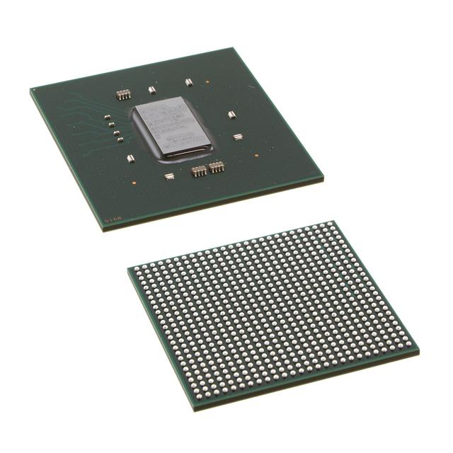
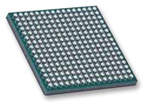
XC7Z030-L2FBG676I
XC7Z030-L2FBG676I ECAD Model
XC7Z030-L2FBG676I Attributes
| Type | Description | Select |
|---|---|---|
| Rohs Code | Yes | |
| Part Life Cycle Code | Active | |
| Surface Mount | YES | |
| Supply Voltage-Nom | 1 V | |
| uPs/uCs/Peripheral ICs Type | SYSTEM ON CHIP | |
| Technology | CMOS | |
| Supply Voltage-Max | 1.05 V | |
| Supply Voltage-Min | 950 mV | |
| JESD-30 Code | S-PBGA-B676 | |
| Operating Temperature-Max | 100 °C | |
| Operating Temperature-Min | -40 °C | |
| Number of Terminals | 676 | |
| Package Body Material | PLASTIC/EPOXY | |
| Package Code | BGA | |
| Package Equivalence Code | BGA676,26X26,40 | |
| Package Shape | SQUARE | |
| Package Style | GRID ARRAY | |
| Terminal Form | BALL | |
| Terminal Pitch | 1 mm | |
| Terminal Position | BOTTOM | |
| Seated Height-Max | 2.54 mm | |
| Width | 27 mm | |
| Length | 27 mm | |
| Ihs Manufacturer | XILINX INC | |
| Package Description | BGA, | |
| Reach Compliance Code | compliant | |
| ECCN Code | 3A991.D | |
| HTS Code | 8542.39.00.01 |
XC7Z030-L2FBG676I Datasheet Download
XC7Z030-L2FBG676I Overview
The XC7Z030-L2FBG676I chip model is a high-performance and high-density programmable logic device (PLD) that has been designed with the intention to provide superior performance and flexibility. It is based on the latest Xilinx 7 series FPGA technology, and is capable of supporting high-speed serial transceivers, advanced memory interfaces, and high-speed I/O. This model has been designed to be used in a wide range of applications such as communications, embedded systems, and industrial automation.
The XC7Z030-L2FBG676I chip model is capable of providing up to 676K logic cells, which are the building blocks for logic functions. This model also supports up to 8GB of RAM, as well as up to 4GB of Flash memory, allowing for the storage of large amounts of data. In addition, this model also supports up to 12 high-speed serial transceivers, allowing for the transmission of data at speeds of up to 12.5 Gbps.
The XC7Z030-L2FBG676I chip model has the potential to be upgraded in the future to meet the needs of more advanced applications. For example, it can be upgraded to support higher speed transceivers, higher resolution displays, or larger memory sizes. It can also be used to develop and popularize future intelligent robots, as it is capable of providing the necessary processing power and flexibility for controlling robotic systems.
In order to use the XC7Z030-L2FBG676I chip model effectively, technical talents with knowledge in FPGA design and embedded systems are necessary. Knowledge of VHDL and Verilog programming languages is also required in order to be able to program the chip properly. Additionally, knowledge of circuit design and debugging techniques are also important in order to be able to troubleshoot any issues that may arise.
Case studies and precautions should also be taken into consideration when using the XC7Z030-L2FBG676I chip model. For example, power consumption should be monitored closely and the chip should be operated within the specified temperature range. Additionally, the chip should be tested and verified before being used in any production environment.
Overall, the XC7Z030-L2FBG676I chip model is a powerful and flexible programmable logic device that has been designed to meet the needs of a wide range of applications. It has the potential to be upgraded in the future to meet the needs of more advanced applications, and can also be used to develop and popularize future intelligent robots. In order to use the model effectively, technical talents with knowledge in FPGA design and embedded systems are necessary, and case studies and precautions should also be taken into consideration.
You May Also Be Interested In

1,875 In Stock
Pricing (USD)
| QTY | Unit Price | Ext Price |
|---|---|---|
| 1+ | $220.4763 | $220.4763 |
| 10+ | $218.1056 | $2,181.0560 |
| 100+ | $206.2520 | $20,625.2031 |
| 1000+ | $194.3985 | $97,199.2330 |
| 10000+ | $177.8035 | $177,803.4750 |
| The price is for reference only, please refer to the actual quotation! | ||