
AMD Xilinx
XC7S100-2FGGA676I
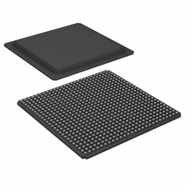
XC7S100-2FGGA676I ECAD Model
XC7S100-2FGGA676I Attributes
| Type | Description | Select |
|---|---|---|
| Mfr | AMD Xilinx | |
| Series | Spartan®-7 | |
| Package | Tray | |
| Number of LABs/CLBs | 8000 | |
| Number of Logic Elements/Cells | 102400 | |
| Total RAM Bits | 4423680 | |
| Number of I/O | 400 | |
| Voltage - Supply | 0.95V ~ 1.05V | |
| Mounting Type | Surface Mount | |
| Operating Temperature | -40°C ~ 100°C (TJ) | |
| Package / Case | 676-BGA | |
| Supplier Device Package | 676-FPBGA (27x27) | |
| Base Product Number | XC7S100 |
XC7S100-2FGGA676I Overview
The XC7S100-2FGGA676I is a FPGA chip from the Xilinx 7 series. It is a high-performance, low-power FPGA chip that is suitable for a variety of applications. It has a capacity of 100K logic cells and 1,536 DSP slices. It has 676 I/O pins, with 8 banks of 88 I/O pins. It also has dedicated clock management circuitry, which can be used to reduce clock jitter and power consumption.
The chip is designed to operate at a maximum clock frequency of 500 MHz. It has a power-efficient architecture, with a power consumption of less than 1.5W. It is also designed to be resistant to electrostatic discharge (ESD) and over-temperature events.
The XC7S100-2FGGA676I is suitable for a wide range of applications, including high-speed networking, communications, and video processing. It can be used for data acquisition, control systems, and embedded systems. It is also suitable for applications such as digital signal processing, image processing, and machine learning.
The chip has a wide range of features, including a high-speed transceiver, block RAM, and distributed RAM. It also has a wide range of peripherals, including Ethernet, USB, and UART. It also has advanced features, such as clock synchronization, power management, and on-chip debugging.
Overall, the XC7S100-2FGGA676I is a powerful and low-power FPGA chip that is suitable for a wide range of applications. It has a wide range of features, including a high-speed transceiver, block RAM, and distributed RAM. It also has advanced features, such as clock synchronization, power management, and on-chip debugging. It is suitable for applications such as high-speed networking, communications, and video processing.
You May Also Be Interested In
4,225 In Stock
Pricing (USD)
| QTY | Unit Price | Ext Price |
|---|---|---|
| 1+ | $167.0248 | $167.0248 |
| 10+ | $165.2289 | $1,652.2887 |
| 100+ | $156.2490 | $15,624.9042 |
| 1000+ | $147.2692 | $73,634.6060 |
| 10000+ | $134.6975 | $134,697.4500 |
| The price is for reference only, please refer to the actual quotation! | ||