AMD Xilinx
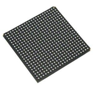
XC7A75T-L1FGG484I
XC7A75T-L1FGG484I ECAD Model
XC7A75T-L1FGG484I Attributes
| Type | Description | Select |
|---|---|---|
| Rohs Code | Yes | |
| Part Life Cycle Code | Active | |
| Supply Voltage-Nom | 950 mV | |
| Number of Inputs | 285 | |
| Number of Outputs | 285 | |
| Number of Logic Cells | 75520 | |
| Number of CLBs | 5900 | |
| Combinatorial Delay of a CLB-Max | 1.27 ns | |
| Programmable Logic Type | FIELD PROGRAMMABLE GATE ARRAY | |
| Package Shape | SQUARE | |
| Organization | 5900 CLBS | |
| Supply Voltage-Max | 980 mV | |
| Supply Voltage-Min | 920 mV | |
| JESD-30 Code | S-PBGA-B484 | |
| JESD-609 Code | e1 | |
| Moisture Sensitivity Level | 3 | |
| Operating Temperature-Max | 100 °C | |
| Operating Temperature-Min | -40 °C | |
| Number of Terminals | 484 | |
| Package Body Material | PLASTIC/EPOXY | |
| Package Code | BGA | |
| Package Shape | SQUARE | |
| Package Style | GRID ARRAY | |
| Surface Mount | YES | |
| Terminal Finish | TIN SILVER COPPER | |
| Terminal Form | BALL | |
| Terminal Pitch | 1 mm | |
| Terminal Position | BOTTOM | |
| Width | 23 mm | |
| Length | 23 mm | |
| Seated Height-Max | 2.6 mm | |
| Ihs Manufacturer | XILINX INC | |
| Package Description | FBGA-484 | |
| Reach Compliance Code | compliant | |
| ECCN Code | 3A991.D | |
| HTS Code | 8542.39.00.01 |
XC7A75T-L1FGG484I Datasheet Download
XC7A75T-L1FGG484I Overview
The XC7A75T-L1FGG484I chip model is a high-performance FPGA designed by Xilinx. It is suitable for a wide range of applications, including high-performance digital signal processing, embedded processing, image processing, and advanced communication systems. It is designed to meet the needs of a wide range of customers for high-performance and low-power solutions.
The XC7A75T-L1FGG484I chip model is designed to be highly scalable and can be customized to fit a variety of needs. Its original design intention was to provide customers with a high-performance, cost-effective solution. It is capable of supporting up to a maximum of 4,000 logic cells, making it suitable for a wide range of applications. It is also designed to be easily upgradeable, allowing customers to upgrade their existing systems with the latest features and capabilities.
The XC7A75T-L1FGG484I chip model is designed to be programmed in HDL (Hardware Description Language). This language allows users to create custom logic designs that can be easily implemented in the FPGA. The chip model also supports a wide range of peripherals, including high-speed serial interfaces, memory controllers, and other peripherals.
In order to ensure that the XC7A75T-L1FGG484I chip model is used correctly, it is important to consider the specific design requirements of the chip model. This includes the power requirements, the number of logic cells, the number of peripherals, and the type of memory controllers. Additionally, it is important to consider the actual case studies and any potential issues that may arise. It is also important to consider the potential for future upgrades to the chip model, as well as any potential compatibility issues.
Overall, the XC7A75T-L1FGG484I chip model is a highly versatile and powerful FPGA. It is designed to provide customers with a high-performance and cost-effective solution, while being easily upgradeable and customizable. It is capable of supporting up to 4,000 logic cells and a wide range of peripherals. Additionally, it is designed to be programmed in HDL, making it suitable for a wide range of applications. Furthermore, it is important to consider the specific design requirements of the chip model, as well as any potential issues that may arise.
You May Also Be Interested In
4,374 In Stock
Pricing (USD)
| QTY | Unit Price | Ext Price |
|---|---|---|
| 1+ | $176.8317 | $176.8317 |
| 10+ | $174.9303 | $1,749.3027 |
| 100+ | $165.4232 | $16,542.3192 |
| 1000+ | $155.9161 | $77,958.0560 |
| 10000+ | $142.6062 | $142,606.2000 |
| The price is for reference only, please refer to the actual quotation! | ||

