
AMD Xilinx
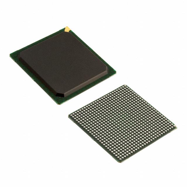
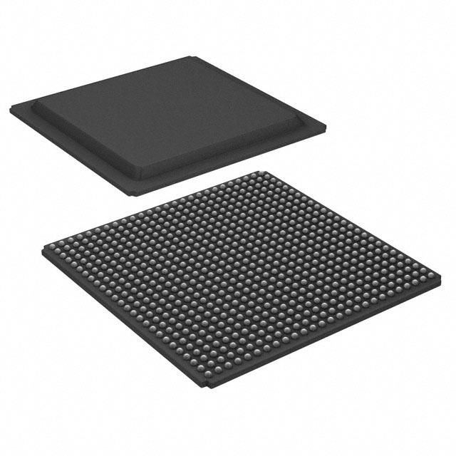
XC6SLX45-2FGG676C
XC6SLX45-2FGG676C ECAD Model
XC6SLX45-2FGG676C Attributes
| Type | Description | Select |
|---|---|---|
| Mfr | AMD Xilinx | |
| Series | Spartan®-6 LX | |
| Package | Tray | |
| Number of LABs/CLBs | 3411 | |
| Number of Logic Elements/Cells | 43661 | |
| Total RAM Bits | 2138112 | |
| Number of I/O | 358 | |
| Voltage - Supply | 1.14V ~ 1.26V | |
| Mounting Type | Surface Mount | |
| Operating Temperature | 0°C ~ 85°C (TJ) | |
| Package / Case | 676-BGA | |
| Supplier Device Package | 676-FBGA (27x27) | |
| Base Product Number | XC6SLX45 |
XC6SLX45-2FGG676C Datasheet Download
XC6SLX45-2FGG676C Overview
The XC6SLX45-2FGG676C is a Field Programmable Gate Array (FPGA) chip model from Xilinx. It is a low-cost, low-power FPGA with a capacity of 45,000 logic cells. It is based on the 6th generation of the Xilinx Spartan-6 FPGA architecture. The chip features 676 I/O pins and a maximum clock frequency of 200 MHz. It has a power dissipation of 1.5 W and a maximum operating temperature of 85°C.
The XC6SLX45-2FGG676C is suitable for a wide range of applications, such as embedded control, image and video processing, automotive, industrial automation, medical imaging, and communications systems. It is also suitable for high-speed serial connectivity and high-speed memory interfaces. The chip supports multiple I/O standards, such as LVDS, LVCMOS, and PCI Express. It also supports multiple power domains, such as core and I/O power domains.
The chip has a number of features that make it suitable for a variety of applications. It supports low-cost and low-power designs, and its 676 I/O pins provide a high degree of flexibility for system design. It also has a wide range of configurable logic blocks, allowing for the implementation of complex designs. It also has a high-speed transceiver block, which supports data rates up to 5 Gbps. Additionally, the chip has a built-in clock management unit, which allows for the implementation of high-speed clock distribution networks.
Overall, the XC6SLX45-2FGG676C is a low-cost, low-power FPGA with a capacity of 45,000 logic cells and 676 I/O pins. It is suitable for a wide range of applications, such as embedded control, image and video processing, automotive, industrial automation, medical imaging, and communications systems. It has a number of features that make it suitable for a variety of applications, such as low-cost and low-power designs, configurable logic blocks, and a high-speed transceiver block.
You May Also Be Interested In
5,997 In Stock
Pricing (USD)
| QTY | Unit Price | Ext Price |
|---|---|---|
| 1+ | $96.1162 | $96.1162 |
| 10+ | $95.0827 | $950.8274 |
| 100+ | $89.9152 | $8,991.5196 |
| 1000+ | $84.7477 | $42,373.8280 |
| 10000+ | $77.5131 | $77,513.1000 |
| The price is for reference only, please refer to the actual quotation! | ||