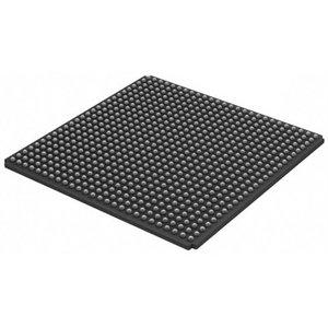
AMD Xilinx
XC6SLX45-2FG676C
XC6SLX45-2FG676C ECAD Model
XC6SLX45-2FG676C Attributes
| Type | Description | Select |
|---|---|---|
| Pbfree Code | No | |
| Rohs Code | No | |
| Part Life Cycle Code | Active | |
| Supply Voltage-Nom | 1.2 V | |
| Number of Inputs | 358 | |
| Number of Outputs | 358 | |
| Number of Logic Cells | 43661 | |
| Number of CLBs | 3411 | |
| Combinatorial Delay of a CLB-Max | 260 ps | |
| Programmable Logic Type | FIELD PROGRAMMABLE GATE ARRAY | |
| Temperature Grade | OTHER | |
| Package Shape | SQUARE | |
| Technology | CMOS | |
| Organization | 3411 CLBS | |
| Clock Frequency-Max | 667 MHz | |
| Power Supplies | 1.2,2.5/3.3 V | |
| Supply Voltage-Max | 1.26 V | |
| Supply Voltage-Min | 1.14 V | |
| JESD-30 Code | S-PBGA-B676 | |
| Qualification Status | Not Qualified | |
| JESD-609 Code | e0 | |
| Moisture Sensitivity Level | 3 | |
| Operating Temperature-Max | 85 °C | |
| Peak Reflow Temperature (Cel) | 225 | |
| Time@Peak Reflow Temperature-Max (s) | 30 | |
| Number of Terminals | 676 | |
| Package Body Material | PLASTIC/EPOXY | |
| Package Code | BGA | |
| Package Equivalence Code | BGA676,26X26,40 | |
| Package Shape | SQUARE | |
| Package Style | GRID ARRAY | |
| Surface Mount | YES | |
| Terminal Finish | TIN LEAD | |
| Terminal Form | BALL | |
| Terminal Pitch | 1 mm | |
| Terminal Position | BOTTOM | |
| Width | 27 mm | |
| Length | 27 mm | |
| Seated Height-Max | 2.44 mm | |
| Ihs Manufacturer | XILINX INC | |
| Part Package Code | BGA | |
| Package Description | 27 X 27 MM, 1 MM PITCH, FBGA-676 | |
| Pin Count | 676 | |
| Reach Compliance Code | not_compliant | |
| ECCN Code | 3A991.D | |
| HTS Code | 8542.39.00.01 |
XC6SLX45-2FG676C Datasheet Download
XC6SLX45-2FG676C Overview
The XC6SLX45-2FG676C chip model is a high-performance FPGA (Field Programmable Gate Array) designed for digital signal processing, embedded processing, and image processing. It is a member of the Spartan-6 family of FPGAs, offering a wide range of features, including a rich set of I/O options, superior performance, and low power consumption. The XC6SLX45-2FG676C is programmed using the high-level HDL (Hardware Description Language) language, which makes it easy to develop and optimize the design.
The XC6SLX45-2FG676C chip model offers a number of advantages over other FPGA models, including improved performance and power efficiency. Its low power consumption makes it suitable for applications that require low power consumption, such as wearable devices and embedded systems. The XC6SLX45-2FG676C also offers a wide range of I/O options, making it suitable for various applications.
The demand for the XC6SLX45-2FG676C chip model is expected to grow in the coming years, driven by the increasing demand for high-performance digital signal processing and embedded processing applications. Furthermore, the XC6SLX45-2FG676C is well-suited for applications in the automotive, industrial, and medical sectors, which are expected to experience significant growth in the near future.
The original design intention of the XC6SLX45-2FG676C chip model was to provide a high-performance, low-power FPGA solution for digital signal processing and embedded processing applications. The chip model is designed to be highly configurable, allowing users to optimize the design for their specific needs. The XC6SLX45-2FG676C is also designed to be expandable and upgradable, allowing users to add new features and capabilities as needed.
In addition to its use in digital signal processing and embedded processing applications, the XC6SLX45-2FG676C chip model is also suitable for advanced communication systems. The chip model is capable of handling high-speed data rates and can be used for high-bandwidth applications such as 5G wireless communication. Furthermore, the XC6SLX45-2FG676C is designed to be highly configurable, making it suitable for a wide range of communication systems.
Overall, the XC6SLX45-2FG676C chip model is a highly versatile FPGA solution with a wide range of applications. It offers a number of advantages, including improved performance and power efficiency, as well as a wide range of I/O options. The XC6SLX45-2FG676C is designed to be highly configurable and upgradable, making it suitable for a wide range of applications, including digital signal processing, embedded processing, image processing, and advanced communication systems. The demand for the chip model is expected to increase in the coming years, driven by the increasing demand for high-performance digital signal processing and embedded processing applications.
You May Also Be Interested In
3,511 In Stock
Pricing (USD)
| QTY | Unit Price | Ext Price |
|---|---|---|
| 1+ | $67.3394 | $67.3394 |
| 10+ | $66.6154 | $666.1536 |
| 100+ | $62.9950 | $6,299.4960 |
| 1000+ | $59.3746 | $29,687.2800 |
| 10000+ | $54.3060 | $54,306.0000 |
| The price is for reference only, please refer to the actual quotation! | ||

