
AMD Xilinx
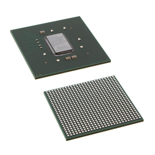
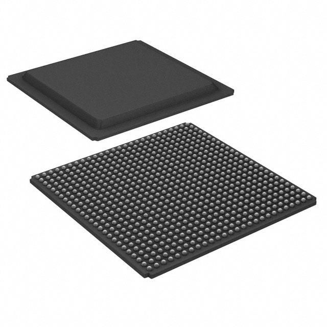
XC5VLX50-1FFG676CES
XC5VLX50-1FFG676CES ECAD Model
XC5VLX50-1FFG676CES Attributes
| Type | Description | Select |
|---|---|---|
| Mfr | AMD Xilinx | |
| Series | Virtex®-5 LX | |
| Package | Tray | |
| Number of LABs/CLBs | 3600 | |
| Number of Logic Elements/Cells | 46080 | |
| Total RAM Bits | 1769472 | |
| Number of I/O | 440 | |
| Voltage - Supply | 0.95V ~ 1.05V | |
| Mounting Type | Surface Mount | |
| Operating Temperature | 0°C ~ 85°C (TJ) | |
| Package / Case | 676-BBGA, FCBGA | |
| Supplier Device Package | 676-FCBGA (27x27) | |
| Base Product Number | XC5VLX50 |
XC5VLX50-1FFG676CES Datasheet Download
XC5VLX50-1FFG676CES Overview
The XC5VLX50-1FFG676CES is a Field Programmable Gate Array (FPGA) chip by Xilinx. It is designed for high-performance, low-cost applications such as industrial automation, automotive, consumer electronics, and communications. The chip features a Virtex-5 LX50 FPGA with 676 logic cells, 50Kbits of distributed RAM, and a maximum clock frequency of 200 MHz. It also has two high-speed transceivers, two Gigabit Ethernet transceivers, and eight RocketIO transceivers.
The chip is designed for low-power applications, with a maximum power consumption of 4.5 W. It has a low-cost package option, allowing for easy integration into existing systems. It also has a wide operating temperature range of -40°C to +85°C, making it suitable for use in harsh environments.
The XC5VLX50-1FFG676CES chip offers a wide range of features, including advanced system-level integration, high-speed transceivers, and low-power operation. It is designed for applications requiring high-performance, low-cost solutions, such as industrial automation, automotive, consumer electronics, and communications. Additionally, the chip can be used for applications such as video processing, medical imaging, and digital signal processing.
You May Also Be Interested In
5,158 In Stock
Pricing (USD)
| QTY | Unit Price | Ext Price |
|---|---|---|
| No reference price found. | ||