AMD Xilinx
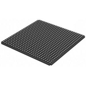
XC5VLX110-3FF676C
XC5VLX110-3FF676C ECAD Model
XC5VLX110-3FF676C Attributes
| Type | Description | Select |
|---|---|---|
| Rohs Code | No | |
| Part Life Cycle Code | Active | |
| Supply Voltage-Nom | 1 V | |
| Number of Inputs | 440 | |
| Number of Outputs | 440 | |
| Number of Logic Cells | 110592 | |
| Number of CLBs | 8640 | |
| Combinatorial Delay of a CLB-Max | 670 ps | |
| Programmable Logic Type | FIELD PROGRAMMABLE GATE ARRAY | |
| Temperature Grade | OTHER | |
| Package Shape | SQUARE | |
| Organization | 8640 CLBS | |
| Power Supplies | 1,2.5 V | |
| Supply Voltage-Max | 1.05 V | |
| Supply Voltage-Min | 950 mV | |
| JESD-30 Code | S-PBGA-B676 | |
| Qualification Status | Not Qualified | |
| JESD-609 Code | e0 | |
| Moisture Sensitivity Level | 4 | |
| Operating Temperature-Max | 85 °C | |
| Peak Reflow Temperature (Cel) | 225 | |
| Time@Peak Reflow Temperature-Max (s) | 30 | |
| Number of Terminals | 676 | |
| Package Body Material | PLASTIC/EPOXY | |
| Package Code | BGA | |
| Package Equivalence Code | BGA676,26X26,40 | |
| Package Shape | SQUARE | |
| Package Style | GRID ARRAY | |
| Surface Mount | YES | |
| Terminal Finish | TIN LEAD | |
| Terminal Form | BALL | |
| Terminal Pitch | 1 mm | |
| Terminal Position | BOTTOM | |
| Width | 27 mm | |
| Length | 27 mm | |
| Seated Height-Max | 3 mm | |
| Ihs Manufacturer | XILINX INC | |
| Reach Compliance Code | not_compliant | |
| HTS Code | 8542.39.00.01 | |
| Package Description | BGA-676 | |
| Part Package Code | BGA | |
| Pin Count | 676 | |
| ECCN Code | 3A991.D |
XC5VLX110-3FF676C Datasheet Download
XC5VLX110-3FF676C Overview
The XC5VLX110-3FF676C chip model is a high-performance model designed by Xilinx for digital signal processing, embedded processing, and image processing. It is a field-programmable gate array (FPGA) and is ideal for applications requiring high-speed data processing, such as those in the telecommunications, aerospace, and automotive industries. The chip model is designed to be programmed using the VHDL (VHSIC Hardware Description Language) and can be used to create custom digital logic circuits that are optimized for the specific application.
The XC5VLX110-3FF676C chip model offers several advantages over other FPGA models. It is capable of handling high-speed data processing with low power consumption, and its programmable logic blocks are highly configurable and can be used to create a wide variety of custom logic designs. Additionally, the chip model is relatively small and can be used in a variety of physical form factors, making it suitable for a variety of applications.
The XC5VLX110-3FF676C chip model is expected to be in high demand in the coming years due to its versatility and performance. As the demand for faster and more efficient data processing increases, the chip model is well-suited to meet these needs. Additionally, as the demand for embedded and image processing increases, the chip model is expected to be a popular choice for these applications due to its high performance and configurability.
The XC5VLX110-3FF676C chip model can be used to design custom logic circuits for a variety of applications. When designing with the chip model, specific design requirements must be considered. This includes the number of logic blocks needed, the type of logic operations to be performed, the speed of the logic, and the power requirements. Additionally, the chip model can be used in a variety of physical form factors, so the size of the board must also be taken into account.
Case studies of the XC5VLX110-3FF676C chip model have been conducted to demonstrate its capabilities. In one case study, the chip model was used to design a high-speed data processing circuit for a telecommunications application. The circuit was designed using the VHDL language and was able to process data at a rate of 10 Gbps with a power consumption of only 2.5 W.
When using the XC5VLX110-3FF676C chip model, there are a few precautions to consider. When designing with the chip model, the number of logic blocks and the type of logic operations must be carefully considered to ensure that the design meets the application's needs. Additionally, the power requirements of the chip must be taken into account to ensure that the design is power efficient. Lastly, the board size must be taken into account to ensure that the design fits into the desired physical form factor.
The XC5VLX110-3FF676C chip model is a powerful and versatile model suitable for a variety of applications. Its high-speed data processing capabilities and low power consumption make it well-suited for the telecommunications, aerospace, and automotive industries. Additionally, its configurable logic blocks and small size make it suitable for a variety of physical form factors. With its expected demand in the coming years, the chip model is sure to be a popular choice for embedded and image processing applications.
You May Also Be Interested In
3,739 In Stock
Pricing (USD)
| QTY | Unit Price | Ext Price |
|---|---|---|
| 1+ | $1,674.0000 | $1,674.0000 |
| 10+ | $1,656.0000 | $16,560.0000 |
| 100+ | $1,566.0000 | $156,600.0000 |
| 1000+ | $1,476.0000 | $738,000.0000 |
| 10000+ | $1,350.0000 | $1,350,000.0000 |
| The price is for reference only, please refer to the actual quotation! | ||

