
AMD Xilinx
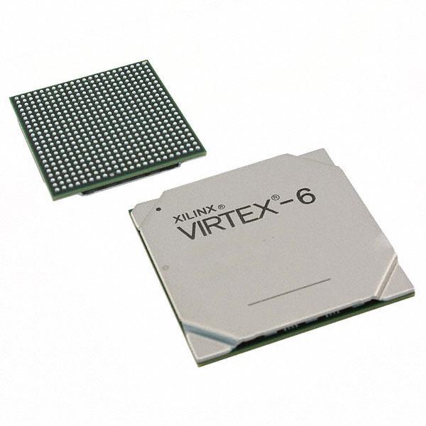
XC5VLX110-2FF1760I
XC5VLX110-2FF1760I ECAD Model
XC5VLX110-2FF1760I Attributes
| Type | Description | Select |
|---|---|---|
| Mfr | AMD Xilinx | |
| Series | Virtex®-5 LX | |
| Package | Tray | |
| Number of LABs/CLBs | 8640 | |
| Number of Logic Elements/Cells | 110592 | |
| Total RAM Bits | 4718592 | |
| Number of I/O | 800 | |
| Voltage - Supply | 0.95V ~ 1.05V | |
| Mounting Type | Surface Mount | |
| Operating Temperature | -40°C ~ 100°C (TJ) | |
| Package / Case | 1760-BBGA, FCBGA | |
| Supplier Device Package | 1760-FCBGA (42.5x42.5) | |
| Base Product Number | XC5VLX110 |
XC5VLX110-2FF1760I Datasheet Download
XC5VLX110-2FF1760I Overview
The XC5VLX110-2FF1760I is a Field Programmable Gate Array (FPGA) chip from Xilinx. It is a Virtex-5 family FPGA with two speed grades, and is based on the Virtex-5 LX110 architecture. This chip has a total of 1760 logic cells, with a total of 110,000 system gates and a maximum of 896 user I/O pins. The device also features a dedicated memory block of 4 Mbits of block RAM, along with 4 DSP slices. It has a total power dissipation of 3.2 W and a total of 3.2 Gb/s of peak data transfer rate.
The XC5VLX110-2FF1760I is suitable for a wide range of applications, including high-speed signal processing, embedded control, high-performance computing, and image processing. It is particularly well-suited for applications that require high-speed signal processing, as it features four DSP slices and a peak data transfer rate of 3.2 Gb/s. Additionally, the device is also suitable for embedded control applications, as it features a dedicated memory block of 4 Mbits of block RAM.
In terms of specifications, the XC5VLX110-2FF1760I is fabricated using a 0.13-micron process and is housed in a 1760-pin FCBGA package. It has a maximum operating frequency of 200 MHz and a maximum I/O voltage of 3.3 V. The device also features a total of 896 user I/O pins, along with four DSP slices and 4 Mbits of block RAM.
Overall, the XC5VLX110-2FF1760I is a powerful FPGA chip from Xilinx, suitable for a wide range of applications. It features a total of 1760 logic cells, with a total of 110,000 system gates and a maximum of 896 user I/O pins. Additionally, it has a maximum operating frequency of 200 MHz and a peak data transfer rate of 3.2 Gb/s. It also features four DSP slices and 4 Mbits of block RAM, making it suitable for high-speed signal processing and embedded control applications.
You May Also Be Interested In


4,718 In Stock
Pricing (USD)
| QTY | Unit Price | Ext Price |
|---|---|---|
| 1+ | $2,422.3226 | $2,422.3226 |
| 10+ | $2,396.2762 | $23,962.7616 |
| 100+ | $2,266.0438 | $226,604.3760 |
| 1000+ | $2,135.8114 | $1,067,905.6800 |
| 10000+ | $1,953.4860 | $1,953,486.0000 |
| The price is for reference only, please refer to the actual quotation! | ||