
AMD Xilinx
XC4013XL-3PQG240I
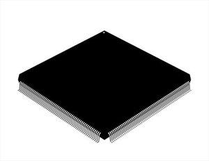
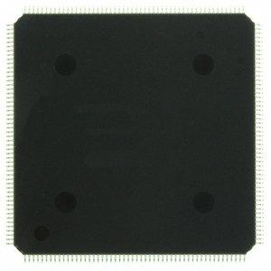
XC4013XL-3PQG240I ECAD Model
XC4013XL-3PQG240I Attributes
| Type | Description | Select |
|---|---|---|
| Pbfree Code | Yes | |
| Rohs Code | Yes | |
| Part Life Cycle Code | Obsolete | |
| Supply Voltage-Nom | 3.3 V | |
| Number of Equivalent Gates | 10000 | |
| Number of CLBs | 576 | |
| Combinatorial Delay of a CLB-Max | 1.6 ns | |
| Programmable Logic Type | FIELD PROGRAMMABLE GATE ARRAY | |
| Package Shape | SQUARE | |
| Technology | CMOS | |
| Organization | 576 CLBS, 10000 GATES | |
| Additional Feature | MAX USABLE 13000 LOGIC GATES | |
| Clock Frequency-Max | 166 MHz | |
| Supply Voltage-Max | 3.6 V | |
| Supply Voltage-Min | 3 V | |
| JESD-30 Code | S-PQFP-G240 | |
| Qualification Status | Not Qualified | |
| JESD-609 Code | e3 | |
| Moisture Sensitivity Level | 3 | |
| Peak Reflow Temperature (Cel) | 245 | |
| Time@Peak Reflow Temperature-Max (s) | 30 | |
| Number of Terminals | 240 | |
| Package Body Material | PLASTIC/EPOXY | |
| Package Code | FQFP | |
| Package Shape | SQUARE | |
| Package Style | FLATPACK, FINE PITCH | |
| Surface Mount | YES | |
| Terminal Finish | Matte Tin (Sn) | |
| Terminal Form | GULL WING | |
| Terminal Pitch | 500 µm | |
| Terminal Position | QUAD | |
| Width | 32 mm | |
| Length | 32 mm | |
| Seated Height-Max | 4.1 mm | |
| Ihs Manufacturer | XILINX INC | |
| Part Package Code | QFP | |
| Package Description | FQFP, | |
| Pin Count | 240 | |
| Reach Compliance Code | compliant | |
| HTS Code | 8542.39.00.01 |
XC4013XL-3PQG240I Datasheet Download
XC4013XL-3PQG240I Overview
The XC4013XL-3PQG240I is a high-performance, low-power field-programmable gate array (FPGA) chip model developed by Xilinx Corporation. It is suitable for a variety of applications, such as digital signal processing, embedded processing, image processing, and advanced communication systems. It is designed to be programmed using the high-level hardware description language (HDL) and offers a wide range of features and capabilities.
The XC4013XL-3PQG240I was designed with the intention of providing a powerful and flexible platform for a variety of applications. It is equipped with an array of programmable logic blocks, which can be used to create custom designs. Additionally, the chip model is equipped with a wide range of I/O and memory interfaces, allowing for the integration of external components, such as memory devices and peripherals.
The XC4013XL-3PQG240I is designed to support future upgrades and expansions. It is equipped with a reconfigurable architecture, which allows for the addition of new features and capabilities. Additionally, the chip model is designed to be compatible with the latest communication protocols, allowing it to be used in advanced communication systems.
When designing with the XC4013XL-3PQG240I, there are a few important considerations to keep in mind. First, it is important to ensure that the design meets the specific requirements of the application. Additionally, it is important to ensure that the design is optimized for the specific application and is able to meet the required performance levels. Additionally, it is important to consider the power and thermal requirements of the design, as these can have a significant impact on the overall performance of the chip model.
To help designers get the most out of the XC4013XL-3PQG240I, Xilinx provides a range of resources, including detailed product descriptions, design examples, and best practices. Additionally, there are a number of case studies available, which provide a detailed look at how the chip model has been used in real-world applications. Finally, Xilinx provides a range of support resources, such as technical documentation and customer support, to help designers get the most out of the chip model.
You May Also Be Interested In
3,270 In Stock
Pricing (USD)
| QTY | Unit Price | Ext Price |
|---|---|---|
| No reference price found. | ||