AMD Xilinx
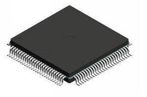
XC4010E-3PQG160I
XC4010E-3PQG160I ECAD Model
XC4010E-3PQG160I Attributes
| Type | Description | Select |
|---|---|---|
| Pbfree Code | Yes | |
| Rohs Code | Yes | |
| Part Life Cycle Code | Obsolete | |
| Supply Voltage-Nom | 5 V | |
| Number of Equivalent Gates | 7000 | |
| Number of CLBs | 400 | |
| Combinatorial Delay of a CLB-Max | 2 ns | |
| Programmable Logic Type | FIELD PROGRAMMABLE GATE ARRAY | |
| Package Shape | SQUARE | |
| Technology | CMOS | |
| Organization | 400 CLBS, 7000 GATES | |
| Additional Feature | MAX USABLE 10000 LOGIC GATES | |
| Clock Frequency-Max | 125 MHz | |
| Supply Voltage-Max | 5.5 V | |
| Supply Voltage-Min | 4.5 V | |
| JESD-30 Code | S-PQFP-G160 | |
| Qualification Status | Not Qualified | |
| JESD-609 Code | e3 | |
| Moisture Sensitivity Level | 3 | |
| Peak Reflow Temperature (Cel) | 245 | |
| Time@Peak Reflow Temperature-Max (s) | 30 | |
| Number of Terminals | 160 | |
| Package Body Material | PLASTIC/EPOXY | |
| Package Code | QFP | |
| Package Shape | SQUARE | |
| Package Style | FLATPACK | |
| Surface Mount | YES | |
| Terminal Finish | MATTE TIN | |
| Terminal Form | GULL WING | |
| Terminal Pitch | 650 µm | |
| Terminal Position | QUAD | |
| Width | 28 mm | |
| Length | 28 mm | |
| Seated Height-Max | 4.1 mm | |
| Ihs Manufacturer | XILINX INC | |
| Part Package Code | QFP | |
| Package Description | QFP, | |
| Pin Count | 160 | |
| Reach Compliance Code | compliant | |
| HTS Code | 8542.39.00.01 |
XC4010E-3PQG160I Datasheet Download
XC4010E-3PQG160I Overview
The Xilinx XC4010E-3PQG160I is a high-performance, low-cost, field-programmable gate array (FPGA) chip model designed for a wide range of applications. It is the latest addition to the Xilinx family of FPGA products and offers a number of advantages over other models. It is a cost-effective solution for high-speed data acquisition and signal processing, and can be used in a variety of applications, including embedded systems, industrial automation, and medical equipment.
The XC4010E-3PQG160I chip model is based on the Virtex-4 FPGA architecture, which provides a high-performance, low-cost solution for digital signal processing and data acquisition. It has a total of 160 logic blocks with 8-bit multipliers and up to 4,096 bits of RAM. The chip also supports a wide range of I/O options, including LVDS, PCI Express, and USB 2.0. The chip also has an integrated clock control unit, which can be used to reduce power consumption and provide better timing control.
The XC4010E-3PQG160I chip model is expected to be in high demand in the future, particularly in the industrial automation and medical equipment industries. The chip’s low cost and high performance make it an ideal choice for these applications. It is also expected to be used in the development of future intelligent robots, as the chip’s low power consumption and high performance make it suitable for use in robotics projects.
To effectively use the XC4010E-3PQG160I chip model, engineers need to be familiar with the Virtex-4 FPGA architecture, as well as with the design and programming of FPGA chips. Knowledge of embedded systems and digital signal processing is also useful, as the chip can be used in a variety of applications. Engineers also need to be familiar with the I/O options available on the chip, as well as with the clock control unit.
In conclusion, the XC4010E-3PQG160I chip model is a high-performance, low-cost solution for digital signal processing and data acquisition. It is expected to be in high demand in the future, particularly in the industrial automation and medical equipment industries. The chip is also suitable for use in the development of future intelligent robots, and engineers need to be familiar with the Virtex-4 FPGA architecture, as well as with the design and programming of FPGA chips, in order to use the chip effectively.
You May Also Be Interested In
1,482 In Stock
Pricing (USD)
| QTY | Unit Price | Ext Price |
|---|---|---|
| No reference price found. | ||
