

AMD Xilinx
XC3S700A-5FGG484I
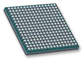
XC3S700A-5FGG484I ECAD Model
XC3S700A-5FGG484I Attributes
| Type | Description | Select |
|---|
XC3S700A-5FGG484I Overview
The Xilinx XC3S700A-5FGG484I is a Field Programmable Gate Array (FPGA) chip model designed by Xilinx Corporation. It is a high-performance, low-power FPGA solution that provides a cost-effective, low-power alternative to traditional ASIC and ASSPs. The XC3S700A-5FGG484I has a wide range of features and capabilities that make it suitable for a variety of applications.
The original design intention of the XC3S700A-5FGG484I was to provide a low-cost, low-power solution for a wide range of applications. It is capable of supporting advanced communication systems, such as high-speed Ethernet and Wi-Fi, as well as other applications such as digital signal processing, image processing, and artificial intelligence. The XC3S700A-5FGG484I is also suitable for the development and popularization of future intelligent robots.
The XC3S700A-5FGG484I is a highly flexible and configurable chip model, allowing users to customize their designs according to their specific requirements. It has high-speed transceivers, memory controllers, and logic blocks that can be configured to meet the needs of the application. The chip also has a wide range of I/O options, including LVDS, LVCMOS, and PCIe.
The XC3S700A-5FGG484I is also capable of future upgrades, allowing users to upgrade their chip models for increased performance and features. This makes the XC3S700A-5FGG484I a great choice for applications that require long-term reliability and scalability.
To ensure that the XC3S700A-5FGG484I is used effectively, users should take into consideration the product description and specific design requirements of the chip model. This includes the power consumption, the number of I/O pins, the speed grade, and the number of logic blocks. It is also important to consider the actual case studies and precautions when using the chip model.
In addition, users should also be aware of the technical talents needed to use the XC3S700A-5FGG484I effectively. Knowledge of FPGA programming, digital signal processing, image processing, and artificial intelligence are all essential for successful implementation of the chip model. Familiarity with the Xilinx Vivado Design Suite and its associated tools is also highly recommended.
In conclusion, the Xilinx XC3S700A-5FGG484I is a powerful, low-power FPGA solution that can be used for a wide range of applications, including advanced communication systems, digital signal processing, image processing, and artificial intelligence. It is capable of future upgrades and is suitable for the development and popularization of future intelligent robots. To use the chip model effectively, users should take into consideration the product description and design requirements, as well as the actual case studies and precautions. Familiarity with the Xilinx Vivado Design Suite and its associated tools is also highly recommended.
You May Also Be Interested In

2,118 In Stock
Pricing (USD)
| QTY | Unit Price | Ext Price |
|---|---|---|
| No reference price found. | ||