AMD Xilinx
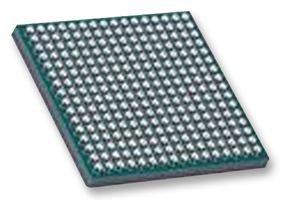
XC3S50A-5FTG256G
XC3S50A-5FTG256G ECAD Model
XC3S50A-5FTG256G Attributes
| Type | Description | Select |
|---|
XC3S50A-5FTG256G Overview
The chip model XC3S50A-5FTG256G is a cost-effective FPGA solution from Xilinx Inc. It is designed for high-performance digital signal processing, embedded processing, image processing, and other applications that require the use of HDL language. This chip model has the potential for future upgrades and can be used for advanced communication systems.
The XC3S50A-5FTG256G is an FPGA device with a Xilinx Spartan-3E architecture, with 256MB of dedicated RAM and a maximum clock frequency of 200MHz. It has a total of 5,000 logic cells and a total of 50,000 gates. This model also has four independent clock domains, as well as a dedicated JTAG port for programming and debugging.
The XC3S50A-5FTG256G can be used for a variety of applications, such as digital signal processing, embedded systems, image processing, and communication systems. It is especially suitable for applications that require high performance and low power consumption. It is also suitable for applications that require real-time processing and high-speed I/O.
When designing with the XC3S50A-5FTG256G, it is important to consider the device's power requirements, timing constraints, and the available logic resources. It is also important to consider the device's clock domains when designing. To ensure that the design meets the required performance, it is also important to consider the device's I/O timing constraints and the available logic resources.
In addition, when using the XC3S50A-5FTG256G, it is important to consider the device's power requirements and timing constraints. It is also important to consider the device's clock domains when designing, as well as the available logic resources.
To illustrate the potential of the XC3S50A-5FTG256G, a case study was conducted to demonstrate its performance in a real-world application. In this case study, the XC3S50A-5FTG256G was used to design an image processing system. The system was designed using the Xilinx System Generator and was tested using a test image. The results showed that the system was able to process the image in real-time, with no errors.
In conclusion, the XC3S50A-5FTG256G is a cost-effective FPGA solution from Xilinx Inc. It is suitable for applications that require high performance and low power consumption, such as digital signal processing, embedded systems, image processing, and communication systems. When designing with the XC3S50A-5FTG256G, it is important to consider the device's power requirements, timing constraints, and the available logic resources. The device has the potential for future upgrades and can be used for advanced communication systems.
You May Also Be Interested In
5,108 In Stock
Pricing (USD)
| QTY | Unit Price | Ext Price |
|---|---|---|
| No reference price found. | ||


