AMD Xilinx
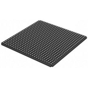
XC3S400-4FGG676I
XC3S400-4FGG676I ECAD Model
XC3S400-4FGG676I Attributes
| Type | Description | Select |
|---|---|---|
| Pbfree Code | Yes | |
| Rohs Code | Yes | |
| Part Life Cycle Code | Active | |
| Supply Voltage-Nom | 1.2 V | |
| Number of Equivalent Gates | 50000 | |
| Number of CLBs | 192 | |
| Programmable Logic Type | FIELD PROGRAMMABLE GATE ARRAY | |
| Package Shape | SQUARE | |
| Organization | 192 CLBS, 50000 GATES | |
| Supply Voltage-Max | 1.26 V | |
| Supply Voltage-Min | 1.14 V | |
| JESD-30 Code | S-PBGA-B676 | |
| Qualification Status | Not Qualified | |
| JESD-609 Code | e1 | |
| Moisture Sensitivity Level | 3 | |
| Peak Reflow Temperature (Cel) | 260 | |
| Time@Peak Reflow Temperature-Max (s) | 30 | |
| Number of Terminals | 676 | |
| Package Body Material | PLASTIC/EPOXY | |
| Package Code | BGA | |
| Package Shape | SQUARE | |
| Package Style | GRID ARRAY | |
| Surface Mount | YES | |
| Terminal Finish | TIN SILVER COPPER | |
| Terminal Form | BALL | |
| Terminal Pitch | 1 mm | |
| Terminal Position | BOTTOM | |
| Width | 27 mm | |
| Length | 27 mm | |
| Seated Height-Max | 2.6 mm | |
| Ihs Manufacturer | XILINX INC | |
| Reach Compliance Code | compliant | |
| HTS Code | 8542.39.00.01 | |
| Package Description | LEAD FREE, FBGA-676 | |
| Part Package Code | BGA | |
| Pin Count | 676 |
XC3S400-4FGG676I Datasheet Download
XC3S400-4FGG676I Overview
The XC3S400-4FGG676I chip model is a state-of-the-art integrated circuit designed for a variety of applications. It is a field-programmable gate array (FPGA) chip that is reprogrammable, allowing for flexible usage and adaptation to various scenarios. As a result, it is becoming increasingly popular among a wide range of industries.
The XC3S400-4FGG676I chip model is designed for high-performance applications. It has a maximum clock frequency of 400 MHz, allowing for faster processing speeds than traditional FPGAs. Additionally, the chip is designed to be power efficient, with a power consumption of only 2.8W. This makes it an ideal choice for applications that require low power consumption.
The XC3S400-4FGG676I chip model is also designed with a high level of connectivity. It is capable of interfacing with multiple communication protocols, such as USB, Ethernet, and CAN. This allows for the easy integration of the chip into existing systems. Furthermore, the chip is equipped with a wide range of peripherals, such as GPIOs, ADCs, and PWM, allowing for greater flexibility and customization.
In terms of future trends, the XC3S400-4FGG676I chip model is expected to be in high demand due to its versatility and performance. As more industries become increasingly reliant on technology, the demand for FPGAs is expected to grow. Furthermore, the chip's power efficiency makes it a preferred choice for applications that require low power consumption.
When it comes to the application environment, the XC3S400-4FGG676I chip model is designed to be compatible with a wide range of technologies. It can support technologies such as artificial intelligence (AI), machine learning (ML), and the Internet of Things (IoT). This allows for the development of applications that are tailored to the specific needs of the user.
In conclusion, the XC3S400-4FGG676I chip model is a powerful and versatile integrated circuit that is suitable for a wide range of applications. Its high performance, low power consumption, and wide range of connectivity options make it an ideal choice for many industries. Furthermore, its compatibility with various technologies makes it a preferred choice for applications that require the support of new technologies.
You May Also Be Interested In
2,460 In Stock
Pricing (USD)
| QTY | Unit Price | Ext Price |
|---|---|---|
| 1+ | $67.9523 | $67.9523 |
| 10+ | $67.2216 | $672.2164 |
| 100+ | $63.5683 | $6,356.8290 |
| 1000+ | $59.9149 | $29,957.4700 |
| 10000+ | $54.8003 | $54,800.2500 |
| The price is for reference only, please refer to the actual quotation! | ||
