

AMD Xilinx
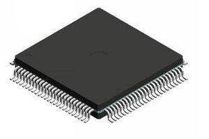
XC3S200-5PQ208
XC3S200-5PQ208 ECAD Model
XC3S200-5PQ208 Attributes
| Type | Description | Select |
|---|
XC3S200-5PQ208 Overview
The Xilinx XC3S200-5PQ208 chip model is a powerful model with a wide range of applications. It is a Field Programmable Gate Array (FPGA) device with a 200-pin PQFP package. This model is a low-cost, low-power, high-performance FPGA solution designed for a variety of applications.
The XC3S200-5PQ208 chip model is designed to meet the needs of a variety of industries, such as automotive, industrial, medical, military, and aerospace. It offers a wide range of features, including on-chip RAM and digital signal processing (DSP) blocks. The chip also supports a variety of I/O standards, such as LVDS, LVCMOS, and CANbus.
In terms of industry trends, the XC3S200-5PQ208 chip model is expected to remain popular in the future. This is due to its low cost, low power consumption, and high performance. Additionally, the chip is highly customizable, allowing users to customize their designs to meet their specific requirements. Furthermore, the chip is highly reliable and has a long product life.
The product description of the XC3S200-5PQ208 chip model includes its power supply voltage, I/O voltage, and maximum clock frequency. Additionally, the chip features a number of built-in features, such as on-chip RAM, DSP blocks, and I/O standards. The chip also offers a wide range of design options, including a variety of I/O standards, programmable logic blocks, and system integration.
In terms of design requirements, the XC3S200-5PQ208 chip model requires careful consideration of the application environment. This includes the power supply voltage, I/O voltage, and maximum clock frequency. Additionally, the design must take into account the I/O standards, programmable logic blocks, and system integration. Furthermore, the design must also consider the reliability and product life of the chip.
In addition to considering the design requirements, the application environment may also require the support of new technologies. This includes technologies such as embedded systems, wireless communication, and artificial intelligence (AI). These technologies can significantly enhance the performance and capabilities of the XC3S200-5PQ208 chip model.
To illustrate the advantages of the XC3S200-5PQ208 chip model, there are a number of case studies and examples. For example, a team of engineers used the XC3S200-5PQ208 chip model to design a low-cost and low-power system for a medical imaging application. The design was successful and the system achieved a high level of performance. Additionally, the team was able to integrate the chip model into the existing system without any major modifications.
Finally, there are a few precautions that should be taken when designing with the XC3S200-5PQ208 chip model. It is important to consider the power supply voltage, I/O voltage, and maximum clock frequency. Additionally, it is important to consider the I/O standards, programmable logic blocks, and system integration. Furthermore, the design must also consider the reliability and product life of the chip.
In conclusion, the XC3S200-5PQ208 chip model is a powerful, low-cost, and low-power FPGA solution designed for a variety of applications. It offers a wide range of features, including on-chip RAM and DSP blocks. Additionally, the chip is highly customizable and is expected to remain popular in the future. When designing with the XC3S200-5PQ208 chip model, it is important to consider the application environment, design requirements, and new technologies. Finally, there are a number of case studies and examples demonstrating the advantages of the chip model.
You May Also Be Interested In
2,204 In Stock
Pricing (USD)
| QTY | Unit Price | Ext Price |
|---|---|---|
| No reference price found. | ||