
AMD Xilinx
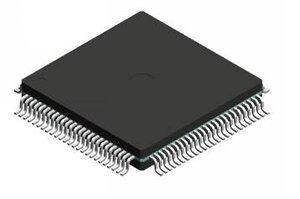
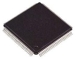
XC3142A-2PQG100C
XC3142A-2PQG100C ECAD Model
XC3142A-2PQG100C Attributes
| Type | Description | Select |
|---|---|---|
| Rohs Code | Yes | |
| Part Life Cycle Code | Obsolete | |
| Supply Voltage-Nom | 5 V | |
| Number of Equivalent Gates | 2000 | |
| Number of CLBs | 144 | |
| Combinatorial Delay of a CLB-Max | 2.2 ns | |
| Programmable Logic Type | FIELD PROGRAMMABLE GATE ARRAY | |
| Temperature Grade | OTHER | |
| Package Shape | RECTANGULAR | |
| Technology | CMOS | |
| Organization | 144 CLBS, 2000 GATES | |
| Additional Feature | MAX USABLE 3000 LOGIC GATES | |
| Clock Frequency-Max | 323 MHz | |
| Supply Voltage-Max | 5.25 V | |
| Supply Voltage-Min | 4.75 V | |
| JESD-30 Code | R-PQFP-G100 | |
| JESD-609 Code | e3 | |
| Moisture Sensitivity Level | 3 | |
| Operating Temperature-Max | 85 °C | |
| Peak Reflow Temperature (Cel) | 245 | |
| Time@Peak Reflow Temperature-Max (s) | 30 | |
| Number of Terminals | 100 | |
| Package Body Material | PLASTIC/EPOXY | |
| Package Code | QFP | |
| Package Shape | RECTANGULAR | |
| Package Style | FLATPACK | |
| Surface Mount | YES | |
| Terminal Finish | MATTE TIN | |
| Terminal Form | GULL WING | |
| Terminal Pitch | 650 µm | |
| Terminal Position | QUAD | |
| Width | 14 mm | |
| Length | 20 mm | |
| Seated Height-Max | 3.4 mm | |
| Ihs Manufacturer | XILINX INC | |
| Part Package Code | QFP | |
| Package Description | QFP, | |
| Pin Count | 100 | |
| Reach Compliance Code | compliant | |
| HTS Code | 8542.39.00.01 |
XC3142A-2PQG100C Datasheet Download
XC3142A-2PQG100C Overview
The Xilinx XC3142A-2PQG100C is a high-performance, low-cost FPGA chip with a wide range of applications. It is suitable for high-performance digital signal processing, embedded processing, image processing, and other applications. Its small size and low power consumption make it ideal for embedded systems. Additionally, it is designed to be programmed in HDL, making it a powerful and versatile tool for FPGA designs.
The XC3142A-2PQG100C has a number of advantages over other FPGA chips. It has a high-speed, low-power architecture that allows for efficient and reliable operation. It also has a high-density logic fabric, allowing for a wide range of applications and designs. Additionally, it is designed to be programmed in HDL, making it easier to design complex logic functions.
The XC3142A-2PQG100C is expected to become increasingly popular in the future, as it is well-suited for the design of high-performance systems. It is also well-suited for embedded systems, as its small size and low power consumption make it ideal for such applications. Additionally, its high-density logic fabric allows for a wide range of designs, making it a powerful tool for FPGA design.
When designing with the XC3142A-2PQG100C, there are a few important considerations. First, the device must be programmed in HDL, as the chip does not support other programming languages. Additionally, the chip must be configured correctly to ensure that it operates correctly. Finally, the design must be tested thoroughly to ensure that it is free of bugs and other issues.
To demonstrate the capabilities of the XC3142A-2PQG100C, we can look at a few case studies. For example, the chip was used to develop an embedded system for controlling a robotic arm. The design used the chip's high-speed, low-power architecture to ensure efficient and reliable operation. Additionally, the chip's high-density logic fabric allowed for the development of complex logic functions.
In conclusion, the Xilinx XC3142A-2PQG100C is a powerful and versatile FPGA chip, well-suited for a wide range of applications. It has a high-speed, low-power architecture, a high-density logic fabric, and is designed to be programmed in HDL. Additionally, its small size and low power consumption make it ideal for embedded systems. As such, it is expected to become increasingly popular in the future, and is a powerful tool for FPGA designs.
You May Also Be Interested In
5,609 In Stock
Pricing (USD)
| QTY | Unit Price | Ext Price |
|---|---|---|
| No reference price found. | ||