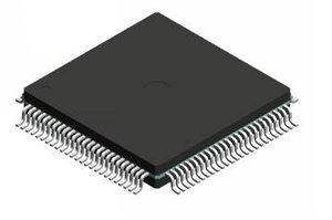
AMD Xilinx
XC3142A-2PQ100I
XC3142A-2PQ100I ECAD Model
XC3142A-2PQ100I Attributes
| Type | Description | Select |
|---|---|---|
| Pbfree Code | No | |
| Rohs Code | No | |
| Part Life Cycle Code | Obsolete | |
| Supply Voltage-Nom | 5 V | |
| Number of Inputs | 82 | |
| Number of Outputs | 82 | |
| Number of Logic Cells | 144 | |
| Number of Equivalent Gates | 2000 | |
| Number of CLBs | 144 | |
| Combinatorial Delay of a CLB-Max | 2.2 ns | |
| Programmable Logic Type | FIELD PROGRAMMABLE GATE ARRAY | |
| Package Shape | RECTANGULAR | |
| Technology | CMOS | |
| Organization | 144 CLBS, 2000 GATES | |
| Additional Feature | MAX USABLE 3000 LOGIC GATES | |
| Clock Frequency-Max | 323 MHz | |
| Power Supplies | 5 V | |
| Supply Voltage-Max | 5.5 V | |
| Supply Voltage-Min | 4.5 V | |
| JESD-30 Code | R-PQFP-G100 | |
| Qualification Status | Not Qualified | |
| JESD-609 Code | e0 | |
| Moisture Sensitivity Level | 3 | |
| Peak Reflow Temperature (Cel) | 225 | |
| Time@Peak Reflow Temperature-Max (s) | 30 | |
| Number of Terminals | 100 | |
| Package Body Material | PLASTIC/EPOXY | |
| Package Code | QFP | |
| Package Equivalence Code | QFP100,.7X.9 | |
| Package Shape | RECTANGULAR | |
| Package Style | FLATPACK | |
| Surface Mount | YES | |
| Terminal Finish | Tin/Lead (Sn85Pb15) | |
| Terminal Form | GULL WING | |
| Terminal Pitch | 650 µm | |
| Terminal Position | QUAD | |
| Width | 14 mm | |
| Length | 20 mm | |
| Seated Height-Max | 3.4 mm | |
| Ihs Manufacturer | XILINX INC | |
| Part Package Code | QFP | |
| Package Description | QFP, QFP100,.7X.9 | |
| Pin Count | 100 | |
| Reach Compliance Code | not_compliant | |
| HTS Code | 8542.39.00.01 |
XC3142A-2PQ100I Datasheet Download
XC3142A-2PQ100I Overview
The XC3142A-2PQ100I chip model is a high-performance digital signal processing, embedded processing, and image processing solution designed by Xilinx. It is designed to meet the needs of multiple applications in a variety of industries. This chip model is based on the Xilinx Virtex-II Pro family of FPGA devices and utilizes the HDL (Hardware Description Language) to program the chip.
The XC3142A-2PQ100I chip model offers several advantages over other chips in the same family. It has a large number of programmable logic cells, allowing for more efficient design of digital signal processing systems. It also has a high degree of flexibility, allowing for the design of complex embedded processing and image processing systems. Additionally, it is capable of operating at high clock speeds, making it suitable for high-performance applications.
The XC3142A-2PQ100I chip model is expected to be in high demand in the coming years due to its unique features and capabilities. It is likely to be used in a variety of industries, including automotive, aerospace, and medical. Additionally, it is likely to be used in advanced communication systems, as it is capable of operating at high clock speeds and provides a high degree of flexibility.
The original design intention of the XC3142A-2PQ100I chip model was to provide a high-performance solution for digital signal processing, embedded processing, and image processing applications. It was designed to be a cost-effective solution that could be easily programmed using the HDL language. The chip model is capable of supporting future upgrades, allowing it to remain relevant in the years to come.
The XC3142A-2PQ100I chip model is a versatile solution that can be used in a variety of applications, including high-performance digital signal processing, embedded processing, and image processing. It is capable of operating at high clock speeds, and its flexibility allows for the design of complex systems. Additionally, it is expected to be in high demand in the coming years, and it is capable of supporting future upgrades. As such, it is likely to be a popular choice for advanced communication systems in the future.
You May Also Be Interested In
1,804 In Stock
Pricing (USD)
| QTY | Unit Price | Ext Price |
|---|---|---|
| No reference price found. | ||

