
AMD Xilinx
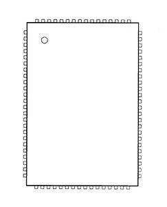
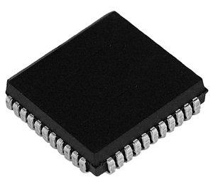
XC3042A-7PCG84I
XC3042A-7PCG84I ECAD Model
XC3042A-7PCG84I Attributes
| Type | Description | Select |
|---|---|---|
| Rohs Code | Yes | |
| Part Life Cycle Code | Obsolete | |
| Supply Voltage-Nom | 5 V | |
| Number of Equivalent Gates | 2000 | |
| Number of CLBs | 144 | |
| Combinatorial Delay of a CLB-Max | 5.1 ns | |
| Programmable Logic Type | FIELD PROGRAMMABLE GATE ARRAY | |
| Package Shape | SQUARE | |
| Technology | CMOS | |
| Organization | 144 CLBS, 2000 GATES | |
| Additional Feature | MAX USABLE 3000 LOGIC GATES | |
| Clock Frequency-Max | 113 MHz | |
| Supply Voltage-Max | 5.5 V | |
| Supply Voltage-Min | 4.5 V | |
| JESD-30 Code | S-PQCC-J84 | |
| JESD-609 Code | e3 | |
| Moisture Sensitivity Level | 3 | |
| Peak Reflow Temperature (Cel) | 245 | |
| Time@Peak Reflow Temperature-Max (s) | 30 | |
| Number of Terminals | 84 | |
| Package Body Material | PLASTIC/EPOXY | |
| Package Code | QCCJ | |
| Package Shape | SQUARE | |
| Package Style | CHIP CARRIER | |
| Surface Mount | YES | |
| Terminal Finish | MATTE TIN | |
| Terminal Form | J BEND | |
| Terminal Pitch | 1.27 mm | |
| Terminal Position | QUAD | |
| Width | 29.3116 mm | |
| Length | 29.3116 mm | |
| Seated Height-Max | 5.08 mm | |
| Ihs Manufacturer | XILINX INC | |
| Part Package Code | LCC | |
| Package Description | QCCJ, | |
| Pin Count | 84 | |
| Reach Compliance Code | compliant | |
| HTS Code | 8542.39.00.01 |
XC3042A-7PCG84I Datasheet Download
XC3042A-7PCG84I Overview
The chip model XC3042A-7PCG84I is a high-performance, low-cost FPGA chip that can be used for a variety of applications. It is designed for digital signal processing, embedded processing, image processing, and other high-performance applications. This chip is designed to be used with the HDL (Hardware Description Language) language, which is used to program the chip and control its behavior.
The original design intention of the XC3042A-7PCG84I was to provide a low-cost, high-performance solution for digital signal processing and other applications. The chip has the capability to be upgraded in the future to support more advanced applications, such as communication systems. It is also designed to be flexible and can be used in a variety of different applications.
The XC3042A-7PCG84I is designed to meet the specific requirements of its users. It has a wide range of features, including high-speed I/O, high-speed memory, and high-speed logic. The chip also has a wide range of peripherals, including USB, Ethernet, and CAN interfaces. It also has a large number of user-configurable options, such as clock speed and power management.
The XC3042A-7PCG84I is a powerful chip that can be used in a variety of applications. To ensure that the chip is used correctly, it is important to understand the product description and design requirements. Additionally, actual case studies and precautions should be taken into account when using the chip. For example, the chip should not be used in high-temperature environments or with high-voltage signals.
In conclusion, the XC3042A-7PCG84I is a powerful, low-cost FPGA chip that can be used for a variety of applications. It is designed for digital signal processing, embedded processing, image processing, and other high-performance applications. The chip is designed to be used with the HDL language, and it has the capability to be upgraded in the future to support more advanced applications. It is important to understand the product description and design requirements of the chip, as well as actual case studies and precautions before using the chip.
You May Also Be Interested In
2,916 In Stock
Pricing (USD)
| QTY | Unit Price | Ext Price |
|---|---|---|
| No reference price found. | ||