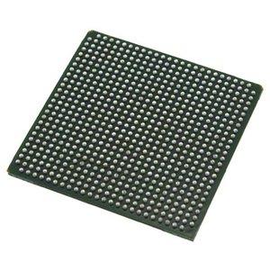
AMD Xilinx
XC2VP4-5FFG672I
XC2VP4-5FFG672I ECAD Model
XC2VP4-5FFG672I Attributes
| Type | Description | Select |
|---|---|---|
| Pbfree Code | Yes | |
| Rohs Code | Yes | |
| Part Life Cycle Code | Obsolete | |
| Supply Voltage-Nom | 1.5 V | |
| Number of Inputs | 348 | |
| Number of Outputs | 348 | |
| Number of Logic Cells | 6768 | |
| Number of CLBs | 752 | |
| Combinatorial Delay of a CLB-Max | 360 ps | |
| Programmable Logic Type | FIELD PROGRAMMABLE GATE ARRAY | |
| Package Shape | SQUARE | |
| Technology | CMOS | |
| Organization | 752 CLBS | |
| Clock Frequency-Max | 1.05 GHz | |
| Power Supplies | 1.5,1.5/3.3,2/2.5,2.5 V | |
| Supply Voltage-Max | 1.575 V | |
| Supply Voltage-Min | 1.425 V | |
| JESD-30 Code | S-PBGA-B672 | |
| Qualification Status | Not Qualified | |
| JESD-609 Code | e1 | |
| Moisture Sensitivity Level | 4 | |
| Peak Reflow Temperature (Cel) | 245 | |
| Time@Peak Reflow Temperature-Max (s) | 30 | |
| Number of Terminals | 672 | |
| Package Body Material | PLASTIC/EPOXY | |
| Package Code | BGA | |
| Package Equivalence Code | BGA672,26X26,40 | |
| Package Shape | SQUARE | |
| Package Style | GRID ARRAY | |
| Surface Mount | YES | |
| Terminal Finish | Tin/Silver/Copper (Sn95.5Ag4.0Cu0.5) | |
| Terminal Form | BALL | |
| Terminal Pitch | 1 mm | |
| Terminal Position | BOTTOM | |
| Width | 27 mm | |
| Length | 27 mm | |
| Seated Height-Max | 2.65 mm | |
| Ihs Manufacturer | XILINX INC | |
| Part Package Code | BGA | |
| Package Description | BGA, BGA672,26X26,40 | |
| Pin Count | 672 | |
| Reach Compliance Code | not_compliant | |
| HTS Code | 8542.39.00.01 | |
| ECCN Code | 3A991.D |
XC2VP4-5FFG672I Datasheet Download
XC2VP4-5FFG672I Overview
The Xilinx XC2VP4-5FFG672I chip model is an FPGA (Field Programmable Gate Array) device that is suitable for a variety of high-performance digital signal processing, embedded processing, and image processing applications. This chip model is a cost-effective, low-power, and programmable solution for these applications, and it requires the use of HDL (Hardware Description Language) for programming.
The XC2VP4-5FFG672I chip model has a number of advantages over other FPGA models. It has a high speed and low power consumption, making it ideal for applications that require fast processing. Additionally, it has a large amount of logic elements, which allows for more complex designs. Finally, the model has a wide range of I/O and memory options, making it suitable for a variety of applications.
The XC2VP4-5FFG672I chip model is expected to see increased demand in the future, as more applications require high-performance digital signal processing, embedded processing, and image processing. Additionally, the product description and specific design requirements of the chip model can be found in the Xilinx documentation.
For those looking to use the XC2VP4-5FFG672I chip model, there are several case studies and precautions to consider. For example, the chip model is not suitable for applications that require large amounts of memory, as it has limited memory options. Additionally, it is important to ensure that the design is optimized to take full advantage of the chip model's features. Finally, it is important to ensure that the HDL code is written correctly, as this is essential for the chip model to work properly.
In conclusion, the Xilinx XC2VP4-5FFG672I chip model is a cost-effective, low-power, and programmable solution for high-performance digital signal processing, embedded processing, and image processing applications. It has a number of advantages over other FPGA models, and it is expected to see increased demand in the future. When using the chip model, it is important to consider the product description and design requirements, as well as case studies and precautions.
You May Also Be Interested In
4,086 In Stock
Pricing (USD)
| QTY | Unit Price | Ext Price |
|---|---|---|
| 1+ | $173.3526 | $173.3526 |
| 10+ | $171.4886 | $1,714.8855 |
| 100+ | $162.1685 | $16,216.8522 |
| 1000+ | $152.8485 | $76,424.2460 |
| 10000+ | $139.8005 | $139,800.4500 |
| The price is for reference only, please refer to the actual quotation! | ||

