
AMD Xilinx
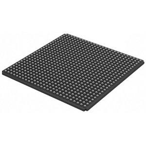
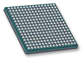
XC2VP30-7FGG676I
XC2VP30-7FGG676I ECAD Model
XC2VP30-7FGG676I Attributes
| Type | Description | Select |
|---|---|---|
| Pbfree Code | Yes | |
| Rohs Code | Yes | |
| Part Life Cycle Code | Obsolete | |
| Supply Voltage-Nom | 1.5 V | |
| Number of CLBs | 3424 | |
| Combinatorial Delay of a CLB-Max | 280 ps | |
| Programmable Logic Type | FIELD PROGRAMMABLE GATE ARRAY | |
| Package Shape | SQUARE | |
| Technology | CMOS | |
| Organization | 3424 CLBS | |
| Clock Frequency-Max | 1.35 GHz | |
| Supply Voltage-Max | 1.575 V | |
| Supply Voltage-Min | 1.425 V | |
| JESD-30 Code | S-PBGA-B676 | |
| Qualification Status | Not Qualified | |
| JESD-609 Code | e1 | |
| Moisture Sensitivity Level | 3 | |
| Peak Reflow Temperature (Cel) | 250 | |
| Time@Peak Reflow Temperature-Max (s) | 30 | |
| Number of Terminals | 676 | |
| Package Body Material | PLASTIC/EPOXY | |
| Package Code | BGA | |
| Package Shape | SQUARE | |
| Package Style | GRID ARRAY | |
| Surface Mount | YES | |
| Terminal Finish | Tin/Silver/Copper (Sn95.5Ag4.0Cu0.5) | |
| Terminal Form | BALL | |
| Terminal Pitch | 1 mm | |
| Terminal Position | BOTTOM | |
| Width | 27 mm | |
| Length | 27 mm | |
| Seated Height-Max | 2.6 mm | |
| Ihs Manufacturer | XILINX INC | |
| Part Package Code | BGA | |
| Package Description | BGA, | |
| Pin Count | 676 | |
| Reach Compliance Code | compliant | |
| HTS Code | 8542.39.00.01 |
XC2VP30-7FGG676I Datasheet Download
XC2VP30-7FGG676I Overview
The XC2VP30-7FGG676I chip model is a powerful and versatile integrated circuit (IC) designed for high-performance digital signal processing, embedded processing, image processing and other applications. It is programmed using the hardware description language (HDL) and can be used to create highly efficient, low-cost solutions for various applications.
The original design intention of the XC2VP30-7FGG676I chip model was to provide a cost-effective and reliable solution for digital signal processing and embedded processing applications. It has the potential to be upgraded in the future to meet the requirements of more advanced communication systems. This could include the ability to process more data faster, as well as the addition of new features and capabilities.
The XC2VP30-7FGG676I chip model is also well-suited for use in networks and for intelligent scenarios. It can be used to create systems that are capable of recognizing patterns and making decisions based on the data they receive. This could include applications such as facial recognition, object detection, and natural language processing. Furthermore, in the era of fully intelligent systems, the XC2VP30-7FGG676I chip model could be used to create autonomous robots and other technologies that are capable of learning and adapting to their environment.
Overall, the XC2VP30-7FGG676I chip model is a powerful and versatile integrated circuit that can be used to create highly efficient, low-cost solutions for various applications. It is well-suited for use in networks and for intelligent scenarios and has the potential to be upgraded in the future to meet the requirements of more advanced communication systems. This makes it an ideal choice for those looking to create powerful and reliable solutions for their digital signal processing, embedded processing and image processing needs.
You May Also Be Interested In

3,918 In Stock
Pricing (USD)
| QTY | Unit Price | Ext Price |
|---|---|---|
| No reference price found. | ||