
AMD Xilinx
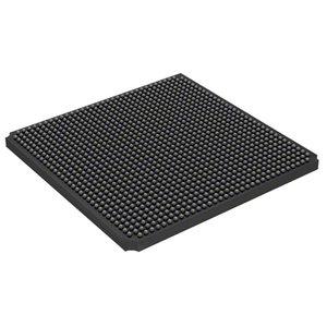
XC2VP30-7FFG1152I
XC2VP30-7FFG1152I ECAD Model
XC2VP30-7FFG1152I Attributes
| Type | Description | Select |
|---|---|---|
| Pbfree Code | Yes | |
| Rohs Code | Yes | |
| Part Life Cycle Code | Obsolete | |
| Supply Voltage-Nom | 1.5 V | |
| Number of CLBs | 3424 | |
| Combinatorial Delay of a CLB-Max | 280 ps | |
| Programmable Logic Type | FIELD PROGRAMMABLE GATE ARRAY | |
| Package Shape | SQUARE | |
| Technology | CMOS | |
| Organization | 3424 CLBS | |
| Clock Frequency-Max | 1.35 GHz | |
| Supply Voltage-Max | 1.575 V | |
| Supply Voltage-Min | 1.425 V | |
| JESD-30 Code | S-PBGA-B1152 | |
| Qualification Status | Not Qualified | |
| JESD-609 Code | e1 | |
| Moisture Sensitivity Level | 4 | |
| Peak Reflow Temperature (Cel) | 245 | |
| Time@Peak Reflow Temperature-Max (s) | 30 | |
| Number of Terminals | 1152 | |
| Package Body Material | PLASTIC/EPOXY | |
| Package Code | BGA | |
| Package Shape | SQUARE | |
| Package Style | GRID ARRAY | |
| Surface Mount | YES | |
| Terminal Finish | Tin/Silver/Copper (Sn95.5Ag4.0Cu0.5) | |
| Terminal Form | BALL | |
| Terminal Pitch | 1 mm | |
| Terminal Position | BOTTOM | |
| Width | 35 mm | |
| Length | 35 mm | |
| Seated Height-Max | 3.4 mm | |
| Ihs Manufacturer | XILINX INC | |
| Part Package Code | BGA | |
| Package Description | 1 MM PITCH, FLIP CHIP, FBGA-1152 | |
| Pin Count | 1152 | |
| Reach Compliance Code | not_compliant | |
| HTS Code | 8542.39.00.01 |
XC2VP30-7FFG1152I Datasheet Download
XC2VP30-7FFG1152I Overview
The Xilinx Virtex-II Pro XC2VP30-7FFG1152I is a Field Programmable Gate Array (FPGA) chip model designed to provide a flexible, high-performance platform for a variety of applications. It is the latest addition to the Virtex-II Pro family, offering a wealth of features and capabilities that make it ideal for a wide range of applications.
The XC2VP30-7FFG1152I is a low-cost, low-power FPGA with a high-speed memory interface, up to 7.5 million system gates, and up to 1.5 million logic cells. It is designed to provide a high-performance, low-cost platform for advanced communication systems. Its features include a high-speed memory interface, up to 7.5 million system gates, and up to 1.5 million logic cells. It also has a built-in system-level test and debug capability, allowing for efficient debugging of complex designs.
The XC2VP30-7FFG1152I is designed to meet the needs of a wide range of applications, including communications, embedded control, video, and image processing. It is also designed to be highly configurable, allowing for easy integration into existing systems. It is capable of supporting a variety of communication protocols, such as Ethernet, USB, and PCI Express. It also supports a range of I/O interfaces, including LVDS, LVCMOS, and SSTL.
In terms of industry trends, the XC2VP30-7FFG1152I is well-positioned to meet the demands of the ever-evolving communications market. It is designed to provide a high-performance, low-cost platform for advanced communication systems. It is also designed to be highly configurable and able to support a range of communication protocols, making it ideal for a variety of applications.
In terms of future development, the XC2VP30-7FFG1152I is designed to be upgradeable, allowing for easy integration of new technologies and features. It is also designed to be highly reliable, offering a long product life cycle and low power consumption. The chip is also designed to be highly configurable, allowing for easy integration into existing systems.
When it comes to product description and design requirements, the XC2VP30-7FFG1152I is designed to meet the needs of a wide range of applications. It is designed to provide a high-performance, low-cost platform for advanced communication systems. Its features include a high-speed memory interface, up to 7.5 million system gates, and up to 1.5 million logic cells. It also has a built-in system-level test and debug capability, allowing for efficient debugging of complex designs.
In terms of actual case studies, the XC2VP30-7FFG1152I has been used in a variety of applications, including communications, embedded control, video, and image processing. In each case, the chip has proven to be reliable and highly configurable, allowing for easy integration into existing systems.
When it comes to precautions, it is important to note that the XC2VP30-7FFG1152I is designed to be upgradeable and highly configurable. As such, it is important to ensure that the chip is properly configured for the application it is intended for. Additionally, it is important to ensure that the chip is properly powered and cooled, as it is designed to operate at high temperatures.
In conclusion, the XC2VP30-7FFG1152I is a low-cost, low-power FPGA with a high-speed memory interface, up to 7.5 million system gates, and up to 1.5 million logic cells. It is designed to provide a high-performance, low-cost platform for advanced communication systems. It is also designed to be highly configurable and able to support a range of communication protocols, making it ideal for a variety of applications. Additionally, it is designed to be upgradeable, allowing for easy integration of new technologies and features. Finally, it is important to ensure that the chip is properly configured for the application it is intended for, and that it is properly powered and cooled.
You May Also Be Interested In
1,711 In Stock
Pricing (USD)
| QTY | Unit Price | Ext Price |
|---|---|---|
| No reference price found. | ||