
AMD Xilinx
XC2V2000-5FG676I
XC2V2000-5FG676I ECAD Model
XC2V2000-5FG676I Attributes
| Type | Description | Select |
|---|---|---|
| Mfr | AMD Xilinx | |
| Series | Virtex®-II | |
| Package | Tray | |
| Number of LABs/CLBs | 2688 | |
| Total RAM Bits | 1032192 | |
| Number of I/O | 456 | |
| Number of Gates | 2000000 | |
| Voltage - Supply | 1.425V ~ 1.575V | |
| Mounting Type | Surface Mount | |
| Operating Temperature | -40°C ~ 100°C (TJ) | |
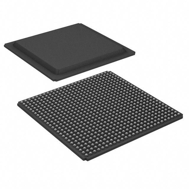
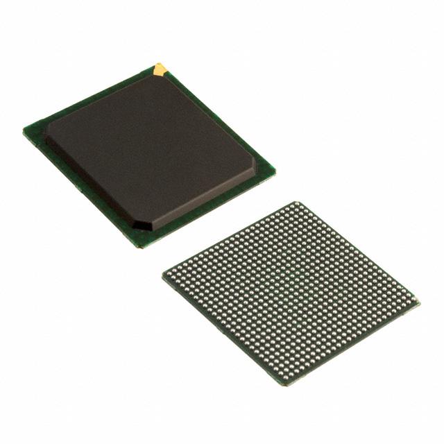
| Package / Case | 676-BGA | |
| Supplier Device Package | 676-FBGA (27x27) | |
| Base Product Number | XC2V2000 |
XC2V2000-5FG676I Datasheet Download
XC2V2000-5FG676I Overview
The XC2V2000-5FG676I is a field-programmable gate array (FPGA) chip model manufactured by Xilinx. It is a 5-volt, low-cost, low-power device that provides high-performance logic and I/O capabilities. The XC2V2000-5FG676I is a high-density, high-performance FPGA with an architecture based on the Virtex-II Pro platform. It features 676 user-configurable logic cells, up to 5.5 Mbits of block RAM, up to 8 DSP slices, up to 144 18x18 multipliers, and up to 48 clock management tiles. It also has up to 1,152 user-configurable I/O pins, including up to 384 LVTTL/LVCMOS, up to 48 differential pairs, up to 48 HSTL, up to 48 SSTL, up to 48 LVDS, and up to 48 PCI-compatible I/O pins.
The XC2V2000-5FG676I is suitable for a wide range of applications, including communications, networking, wireless, automotive, industrial, and consumer applications. It has been designed to provide maximum performance and flexibility for a wide range of applications. It can be used for a variety of tasks, such as high-speed data transfer, high-speed signal processing, and high-speed memory access. It can also be used for high-performance computing, high-speed networking, and high-speed image processing. The XC2V2000-5FG676I is a powerful and flexible FPGA device that can be used in a variety of applications.
You May Also Be Interested In
1,495 In Stock
Pricing (USD)
| QTY | Unit Price | Ext Price |
|---|---|---|
| No reference price found. | ||