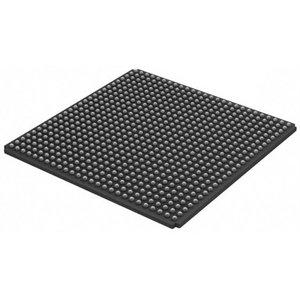
AMD Xilinx
XC2V1500-6FGG676I
XC2V1500-6FGG676I ECAD Model
XC2V1500-6FGG676I Attributes
| Type | Description | Select |
|---|---|---|
| Pbfree Code | Yes | |
| Rohs Code | Yes | |
| Part Life Cycle Code | Obsolete | |
| Supply Voltage-Nom | 1.5 V | |
| Number of Inputs | 392 | |
| Number of Outputs | 392 | |
| Number of Logic Cells | 17280 | |
| Number of Equivalent Gates | 1500000 | |
| Number of CLBs | 1920 | |
| Combinatorial Delay of a CLB-Max | 350 ps | |
| Programmable Logic Type | FIELD PROGRAMMABLE GATE ARRAY | |
| Package Shape | SQUARE | |
| Technology | CMOS | |
| Organization | 1920 CLBS, 1500000 GATES | |
| Clock Frequency-Max | 820 MHz | |
| Power Supplies | 1.5,1.5/3.3,3.3 V | |
| Supply Voltage-Max | 1.575 V | |
| Supply Voltage-Min | 1.425 V | |
| JESD-30 Code | S-PBGA-B676 | |
| Qualification Status | Not Qualified | |
| JESD-609 Code | e1 | |
| Moisture Sensitivity Level | 3 | |
| Peak Reflow Temperature (Cel) | 250 | |
| Time@Peak Reflow Temperature-Max (s) | 30 | |
| Number of Terminals | 676 | |
| Package Body Material | PLASTIC/EPOXY | |
| Package Code | BGA | |
| Package Equivalence Code | BGA676,26X26,40 | |
| Package Shape | SQUARE | |
| Package Style | GRID ARRAY | |
| Surface Mount | YES | |
| Terminal Finish | Tin/Silver/Copper (Sn95.5Ag4.0Cu0.5) | |
| Terminal Form | BALL | |
| Terminal Pitch | 1 mm | |
| Terminal Position | BOTTOM | |
| Width | 27 mm | |
| Length | 27 mm | |
| Seated Height-Max | 2.6 mm | |
| Ihs Manufacturer | XILINX INC | |
| Part Package Code | BGA | |
| Package Description | BGA, BGA676,26X26,40 | |
| Pin Count | 676 | |
| Reach Compliance Code | compliant | |
| HTS Code | 8542.39.00.01 |
XC2V1500-6FGG676I Datasheet Download
XC2V1500-6FGG676I Overview
The chip model XC2V1500-6FGG676I is a highly advanced and powerful Integrated Circuit (IC) designed to meet the needs of a wide range of application environments. It is a member of the Xilinx Virtex-II family of Field Programmable Gate Arrays (FPGAs), and is one of the most powerful and versatile ICs available today.
The XC2V1500-6FGG676I is designed to provide a high-performance, low-cost solution for a variety of applications. It provides a wide range of features, including high-speed I/O, multiple clock domains, and advanced logic synthesis capabilities. The chip also has a number of power management features, including dynamic voltage scaling and power-down modes.
The XC2V1500-6FGG676I is designed to provide a low-cost solution for a variety of applications, including high-speed networking, embedded systems, and industrial automation. It is also suitable for use in high-end consumer electronics, such as digital cameras and camcorders.
In terms of industry trends, the XC2V1500-6FGG676I is expected to be in high demand in the coming years. This is due to its low cost, high performance, and wide range of features. It is also expected to be in high demand in the automotive and aerospace industries, due to its high-speed I/O and power management features.
The XC2V1500-6FGG676I is designed to meet the specific needs of various application environments. It is capable of supporting a wide range of technologies, including DDR3, QDRII, and SERDES. It also supports high-speed I/O, multiple clock domains, and advanced logic synthesis capabilities.
When designing with the XC2V1500-6FGG676I, it is important to consider the specific requirements of the application environment. This includes the power requirements, the number of I/O pins, and the specific features needed. It is also important to consider the specific design requirements of the chip, such as the number of logic cells, the number of I/O pins, and the number of clock domains.
In order to ensure the reliable operation of the chip, it is important to consider the specific design requirements of the application environment. This includes the power requirements, the number of I/O pins, and the specific features needed. It is also important to consider the specific design requirements of the chip, such as the number of logic cells, the number of I/O pins, and the number of clock domains.
When designing with the XC2V1500-6FGG676I, it is important to consider the specific requirements of the application environment. It is also important to consider the specific design requirements of the chip, such as the number of logic cells, the number of I/O pins, and the number of clock domains. It is also important to consider the specific design requirements of the application environment, such as the power requirements, the number of I/O pins, and the specific features needed.
The XC2V1500-6FGG676I is a powerful and versatile IC that is expected to be in high demand in the coming years. It is designed to provide a low-cost solution for a variety of applications. It is also capable of supporting a wide range of technologies, including DDR3, QDRII, and SERDES. When designing with the XC2V1500-6FGG676I, it is important to consider the specific requirements of the application environment, as well as the specific design requirements of the chip. By doing so, designers can ensure that the chip is able to meet the needs of their application environment and provide reliable performance.
You May Also Be Interested In
1,292 In Stock
Pricing (USD)
| QTY | Unit Price | Ext Price |
|---|---|---|
| No reference price found. | ||

