
AMD Xilinx
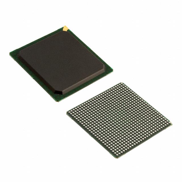
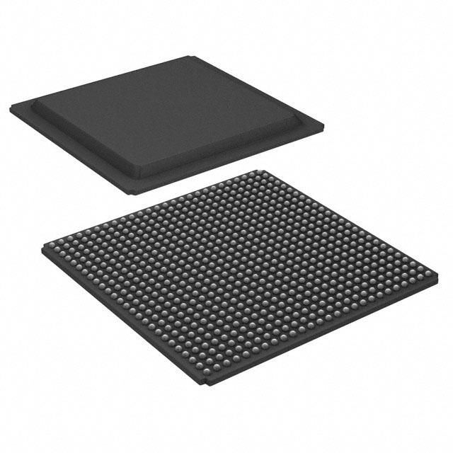
XC2V1500-4FGG676I
XC2V1500-4FGG676I ECAD Model
XC2V1500-4FGG676I Attributes
| Type | Description | Select |
|---|---|---|
| Mfr | AMD Xilinx | |
| Series | Virtex®-II | |
| Package | Tray | |
| Number of LABs/CLBs | 1920 | |
| Total RAM Bits | 884736 | |
| Number of I/O | 392 | |
| Number of Gates | 1500000 | |
| Voltage - Supply | 1.425V ~ 1.575V | |
| Mounting Type | Surface Mount | |
| Operating Temperature | -40°C ~ 100°C (TJ) | |
| Package / Case | 676-BGA | |
| Supplier Device Package | 676-FBGA (27x27) | |
| Base Product Number | XC2V1500 |
XC2V1500-4FGG676I Datasheet Download
XC2V1500-4FGG676I Overview
The XC2V1500-4FGG676I is a Field Programmable Gate Array (FPGA) chip manufactured by Xilinx. It is a low-cost, high-performance device designed for a wide range of applications. It is part of the Virtex-II family of FPGAs and is available in a 4-layer, 676-pin, Flip-Chip Ball Grid Array (FBGA) package.
The XC2V1500-4FGG676I has a total of 4 million system gates, and can support up to 150Kbits of distributed RAM. It also offers up to 1536 user I/O pins, with the ability to support up to four independent clock domains. It also has two dedicated clock pins for external clock sources.
The XC2V1500-4FGG676I can be used in a variety of applications, such as digital signal processing, embedded systems, communications, industrial automation, and more. It is ideal for applications that require high performance and low power consumption, as it has a maximum power dissipation of 4.5W. It also offers a wide range of features, such as on-chip clock management, high-speed transceivers, and a dedicated JTAG port for debugging.
Overall, the XC2V1500-4FGG676I is a powerful and versatile FPGA chip that can be used in a variety of applications. It offers high performance, low power consumption, and a wide range of features, making it an ideal choice for many different applications.
You May Also Be Interested In
3,776 In Stock
Pricing (USD)
| QTY | Unit Price | Ext Price |
|---|---|---|
| No reference price found. | ||