

AMD Xilinx
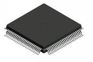
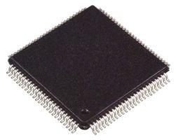
XC2S400E-7FGG456I
XC2S400E-7FGG456I ECAD Model
XC2S400E-7FGG456I Attributes
| Type | Description | Select |
|---|
XC2S400E-7FGG456I Overview
The chip model XC2S400E-7FGG456I is a powerful and reliable integrated circuit (IC) designed to meet the needs of a variety of applications. It is a Field Programmable Gate Array (FPGA) device with an impressive feature set, including four-input look-up tables (LUTs), embedded block RAM, and digital signal processing (DSP) blocks. It is also equipped with a range of I/O options and a high-performance, low-power, low-cost architecture.
The XC2S400E-7FGG456I is built with the latest technologies to ensure that it can meet the needs of the most demanding applications. It features a high-speed transceiver, multi-gigabit transceivers, and high-speed I/O, as well as a wide range of clock management options. It also offers advanced features such as power-on reset, programmable clock dividers, and programmable clock gating, making it an ideal choice for a variety of applications.
In terms of industry trends, the XC2S400E-7FGG456I is expected to be in high demand in the future. As more applications require the use of FPGAs, the demand for the XC2S400E-7FGG456I is expected to increase. This is due to its wide range of features and its competitive price point. It is also expected to be widely used in the automotive, industrial, and medical industries, as well as in the consumer electronics market.
In terms of product description, the XC2S400E-7FGG456I is a highly integrated FPGA device with a range of features, including four-input look-up tables (LUTs), embedded block RAM, and digital signal processing (DSP) blocks. It also has a wide range of I/O options and a high-performance, low-power, low-cost architecture. Its transceiver and multi-gigabit transceivers offer advanced features such as power-on reset, programmable clock dividers, and programmable clock gating.
In terms of design requirements, the XC2S400E-7FGG456I is designed to be a reliable and cost-effective solution for a variety of applications. It is designed to meet the needs of a variety of applications, including automotive, industrial, medical, and consumer electronics. Its wide range of features and competitive price point make it an ideal choice for many applications.
In terms of actual case studies, the XC2S400E-7FGG456I has been used in a variety of applications, including the automotive, industrial, medical, and consumer electronics markets. It has been used in a wide range of applications, including automotive control systems, industrial automation, medical imaging, and consumer electronics.
In terms of precautions, the XC2S400E-7FGG456I should be used with caution in applications that require high-speed or high-power operation. It is important to ensure that the device is properly configured and that the appropriate safety measures are taken to ensure that the device is not damaged.
In conclusion, the XC2S400E-7FGG456I is a powerful and reliable integrated circuit (IC) designed to meet the needs of a variety of applications. It is expected to be in high demand in the future due to its wide range of features and competitive price point. It is designed to be a reliable and cost-effective solution for a variety of applications, including automotive, industrial, medical, and consumer electronics. In order to ensure the best results, it is important to ensure that the device is properly configured and that the appropriate safety measures are taken to ensure that the device is not damaged.
You May Also Be Interested In
1,549 In Stock
Pricing (USD)
| QTY | Unit Price | Ext Price |
|---|---|---|
| No reference price found. | ||