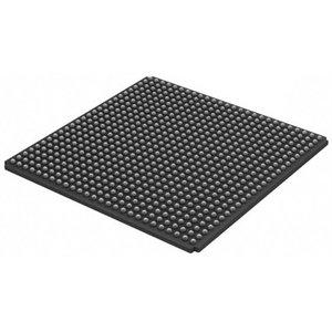
AMD Xilinx
XC2S400E-6FGG676I
XC2S400E-6FGG676I ECAD Model
XC2S400E-6FGG676I Attributes
| Type | Description | Select |
|---|---|---|
| Pbfree Code | Yes | |
| Rohs Code | Yes | |
| Part Life Cycle Code | Obsolete | |
| Supply Voltage-Nom | 1.8 V | |
| Number of Inputs | 410 | |
| Number of Outputs | 410 | |
| Number of Logic Cells | 10800 | |
| Number of Equivalent Gates | 52000 | |
| Number of CLBs | 864 | |
| Combinatorial Delay of a CLB-Max | 470 ps | |
| Programmable Logic Type | FIELD PROGRAMMABLE GATE ARRAY | |
| Package Shape | SQUARE | |
| Technology | CMOS | |
| Organization | 864 CLBS, 52000 GATES | |
| Additional Feature | MAXIMUM USABLE GATES = 150000 | |
| Clock Frequency-Max | 357 MHz | |
| Power Supplies | 1.2/3.6,1.8 V | |
| Supply Voltage-Max | 1.89 V | |
| Supply Voltage-Min | 1.71 V | |
| JESD-30 Code | S-PBGA-B676 | |
| Qualification Status | Not Qualified | |
| JESD-609 Code | e1 | |
| Moisture Sensitivity Level | 3 | |
| Peak Reflow Temperature (Cel) | 250 | |
| Time@Peak Reflow Temperature-Max (s) | 30 | |
| Number of Terminals | 676 | |
| Package Body Material | PLASTIC/EPOXY | |
| Package Code | BGA | |
| Package Equivalence Code | BGA676,26X26,40 | |
| Package Shape | SQUARE | |
| Package Style | GRID ARRAY | |
| Surface Mount | YES | |
| Terminal Finish | Tin/Silver/Copper (Sn95.5Ag4.0Cu0.5) | |
| Terminal Form | BALL | |
| Terminal Pitch | 1 mm | |
| Terminal Position | BOTTOM | |
| Width | 27 mm | |
| Length | 27 mm | |
| Seated Height-Max | 2.6 mm | |
| Ihs Manufacturer | XILINX INC | |
| Part Package Code | BGA | |
| Package Description | LEAD FREE, FBGA-676 | |
| Pin Count | 676 | |
| Reach Compliance Code | unknown | |
| ECCN Code | 3A991.D | |
| HTS Code | 8542.39.00.01 |
XC2S400E-6FGG676I Datasheet Download
XC2S400E-6FGG676I Overview
The chip model XC2S400E-6FGG676I is a powerful and versatile FPGA chip designed for a wide range of applications. Its original design intention was to provide an efficient, cost-effective solution for a variety of tasks, including advanced communication systems. It is also capable of being upgraded to meet the demands of future technologies, making it an ideal choice for networks and intelligent scenarios.
In terms of product description, the XC2S400E-6FGG676I is a high-performance FPGA device that integrates multiple high-speed transceivers, a high-performance embedded processor, and a programmable logic array. It is also equipped with up to 400K logic cells, up to 8.5Mbits of block RAM, and up to 8.5Gbps transceivers, making it suitable for a wide variety of applications.
In terms of actual case studies, the XC2S400E-6FGG676I has been used in a variety of applications, including wireless communication, medical imaging, and industrial automation. In particular, it has been used in wireless communication systems to provide a reliable and cost-effective solution for high-speed data transmission. Additionally, it has also been used in medical imaging systems to provide high-resolution images and accurate data for diagnosis and treatment.
Finally, there are some precautions to keep in mind when using the XC2S400E-6FGG676I. For example, it is important to ensure that the system is properly designed and configured to meet the design requirements of the chip. Additionally, it is important to keep in mind that the chip may not be compatible with certain advanced communication systems, and it may require additional upgrades to be compatible with them.
Overall, the XC2S400E-6FGG676I is a powerful and versatile FPGA chip that can be used in a variety of applications. It is capable of being upgraded to meet the demands of future technologies, making it an ideal choice for networks and intelligent scenarios. With proper design and configuration, it can provide a reliable and cost-effective solution for a variety of tasks, including advanced communication systems.
You May Also Be Interested In
2,440 In Stock
Pricing (USD)
| QTY | Unit Price | Ext Price |
|---|---|---|
| No reference price found. | ||
