
Microchip Technology Inc
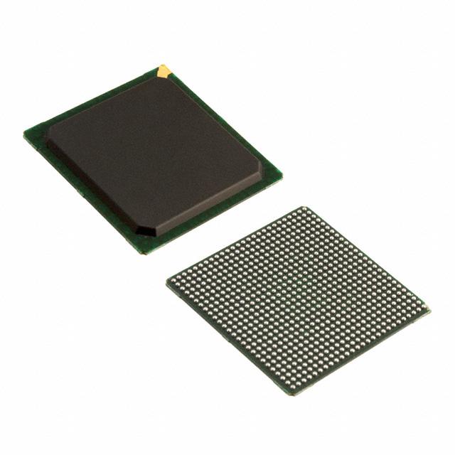
M1A3PE1500-2FGG676
M1A3PE1500-2FGG676 ECAD Model
M1A3PE1500-2FGG676 Attributes
| Type | Description | Select |
|---|---|---|
| Rohs Code | Yes | |
| Part Life Cycle Code | Transferred | |
| Supply Voltage-Nom | 1.5 V | |
| Number of Inputs | 444 | |
| Number of Outputs | 444 | |
| Number of Logic Cells | 38400 | |
| Number of Equivalent Gates | 1500000 | |
| Number of CLBs | 38400 | |
| Programmable Logic Type | FIELD PROGRAMMABLE GATE ARRAY | |
| Temperature Grade | COMMERCIAL | |
| Package Shape | SQUARE | |
| Technology | CMOS | |
| Organization | 38400 CLBS, 1500000 GATES | |
| Clock Frequency-Max | 350 MHz | |
| Power Supplies | 1.5/3.3 V | |
| Supply Voltage-Max | 1.575 V | |
| Supply Voltage-Min | 1.425 V | |
| JESD-30 Code | S-PBGA-B676 | |
| Qualification Status | Not Qualified | |
| JESD-609 Code | e1 | |
| Moisture Sensitivity Level | 3 | |
| Operating Temperature-Max | 70 °C | |
| Peak Reflow Temperature (Cel) | 250 | |
| Time@Peak Reflow Temperature-Max (s) | 30 | |
| Number of Terminals | 676 | |
| Package Body Material | PLASTIC/EPOXY | |
| Package Code | BGA | |
| Package Equivalence Code | BGA676,26X26,40 | |
| Package Shape | SQUARE | |
| Package Style | GRID ARRAY | |
| Surface Mount | YES | |
| Terminal Finish | TIN SILVER COPPER | |
| Terminal Form | BALL | |
| Terminal Pitch | 1 mm | |
| Terminal Position | BOTTOM | |
| Width | 27 mm | |
| Length | 27 mm | |
| Seated Height-Max | 2.44 mm | |
| Ihs Manufacturer | MICROSEMI CORP | |
| Package Description | BGA, BGA676,26X26,40 | |
| Reach Compliance Code | compliant | |
| HTS Code | 8542.39.00.01 |
M1A3PE1500-2FGG676 Datasheet Download
M1A3PE1500-2FGG676 Overview
The M1A3PE1500-2FGG676 is a field-programmable gate array (FPGA) chip manufactured by Altera Corporation. It is a high-performance, low-power device suitable for a variety of applications. The chip features a total of 1500 logic elements, with a maximum clock frequency of 676 MHz. It has a total of 676 I/Os, with a total power consumption of 4.2 W.
The chip is designed to be used in a wide range of applications including digital signal processing, communication systems, embedded systems, and image processing. It is capable of implementing complex logic functions, such as digital filters, signal processing algorithms, and encryption algorithms. It also supports a variety of interfaces such as Ethernet, USB, Serial ATA, and PCI Express.
The chip is designed for easy integration into a variety of systems. It is compatible with Altera’s Quartus II design software, allowing users to easily create and implement their own designs. It also has an on-chip debug system, which allows users to debug their designs in real-time.
Overall, the M1A3PE1500-2FGG676 is a high-performance, low-power FPGA chip suitable for a variety of applications. It offers a total of 1500 logic elements, 676 I/Os, and a maximum clock frequency of 676 MHz. It is compatible with Altera’s Quartus II design software and features an on-chip debug system, making it easy to integrate into a variety of systems.
You May Also Be Interested In

2,356 In Stock
Pricing (USD)
| QTY | Unit Price | Ext Price |
|---|---|---|
| 1+ | $286.4246 | $286.4246 |
| 10+ | $283.3447 | $2,833.4473 |
| 100+ | $267.9456 | $26,794.5558 |
| 1000+ | $252.5464 | $126,273.1940 |
| 10000+ | $230.9876 | $230,987.5500 |
| The price is for reference only, please refer to the actual quotation! | ||