
Microchip Technology Inc
M1A3P400-FGG144
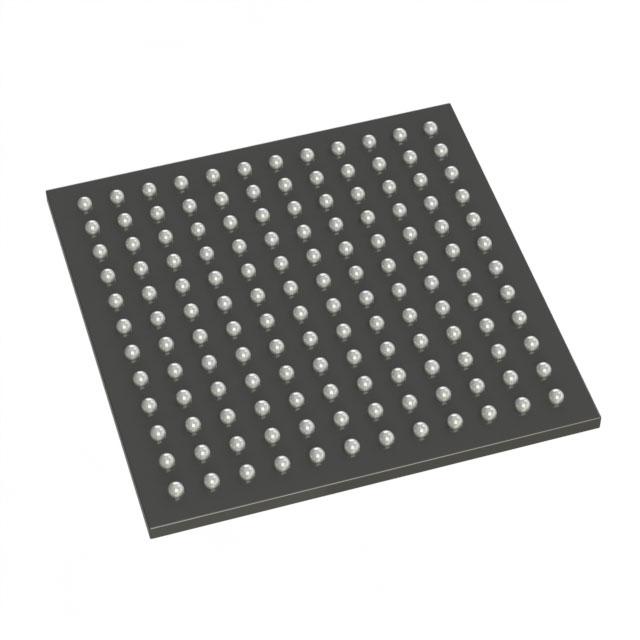
M1A3P400-FGG144 ECAD Model
M1A3P400-FGG144 Attributes
| Type | Description | Select |
|---|---|---|
| Rohs Code | Yes | |
| Part Life Cycle Code | Transferred | |
| Supply Voltage-Nom | 1.5 V | |
| Number of Equivalent Gates | 400000 | |
| Number of CLBs | 9216 | |
| Programmable Logic Type | FIELD PROGRAMMABLE GATE ARRAY | |
| Temperature Grade | COMMERCIAL | |
| Package Shape | SQUARE | |
| Technology | CMOS | |
| Organization | 9216 CLBS, 400000 GATES | |
| Clock Frequency-Max | 350 MHz | |
| Supply Voltage-Max | 1.575 V | |
| Supply Voltage-Min | 1.425 V | |
| JESD-30 Code | S-PBGA-B144 | |
| Qualification Status | Not Qualified | |
| JESD-609 Code | e1 | |
| Moisture Sensitivity Level | 3 | |
| Operating Temperature-Max | 85 °C | |
| Peak Reflow Temperature (Cel) | 260 | |
| Time@Peak Reflow Temperature-Max (s) | 30 | |
| Number of Terminals | 144 | |
| Package Body Material | PLASTIC/EPOXY | |
| Package Code | LBGA | |
| Package Shape | SQUARE | |
| Package Style | GRID ARRAY, LOW PROFILE | |
| Surface Mount | YES | |
| Terminal Finish | TIN SILVER COPPER | |
| Terminal Form | BALL | |
| Terminal Pitch | 1 mm | |
| Terminal Position | BOTTOM | |
| Width | 13 mm | |
| Length | 13 mm | |
| Seated Height-Max | 1.55 mm | |
| Ihs Manufacturer | MICROSEMI CORP | |
| Package Description | LBGA, | |
| Reach Compliance Code | compliant | |
| HTS Code | 8542.39.00.01 |
M1A3P400-FGG144 Datasheet Download
M1A3P400-FGG144 Overview
The M1A3P400-FGG144 is an advanced Field Programmable Gate Array (FPGA) chip from Xilinx, Inc. It is a high-performance, low-power, and highly integrated device that is suitable for a wide range of applications.
The M1A3P400-FGG144 is a 3.3V device with a total of 400K logic cells and 4.5Mbits of embedded memory. It has a total of 144 I/O pins and up to 1150 user I/O signals. The device also supports up to 5 clock domains and has a maximum operating frequency of 250MHz.
The chip is designed to provide high-performance and low-power operation. It features a low-power static phase-locked loop (PLL) and clock-domain crossing (CDC) capabilities that enable faster and more efficient communication between multiple clock domains. The chip also has a wide range of advanced features such as high-speed transceivers, advanced power management, and advanced error correction.
The M1A3P400-FGG144 is suitable for a wide range of applications such as high-speed networking, video processing, embedded systems, and automotive applications. It is also well-suited for high-performance computing and data processing applications.
Overall, the M1A3P400-FGG144 is an advanced FPGA chip from Xilinx, Inc. that provides high-performance and low-power operation. It has a wide range of advanced features and is suitable for a wide range of applications.
You May Also Be Interested In

2,774 In Stock
Pricing (USD)
| QTY | Unit Price | Ext Price |
|---|---|---|
| 1+ | $29.4559 | $29.4559 |
| 10+ | $29.1392 | $291.3916 |
| 100+ | $27.5555 | $2,755.5510 |
| 1000+ | $25.9719 | $12,985.9300 |
| 10000+ | $23.7548 | $23,754.7500 |
| The price is for reference only, please refer to the actual quotation! | ||