
Microchip Technology Inc
M1A3P250-FG144
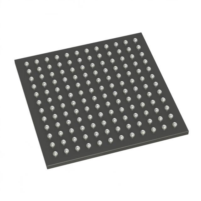
M1A3P250-FG144 ECAD Model
M1A3P250-FG144 Attributes
| Type | Description | Select |
|---|---|---|
| Rohs Code | No | |
| Part Life Cycle Code | Transferred | |
| Supply Voltage-Nom | 1.5 V | |
| Number of Equivalent Gates | 250000 | |
| Number of CLBs | 6144 | |
| Programmable Logic Type | FIELD PROGRAMMABLE GATE ARRAY | |
| Temperature Grade | COMMERCIAL | |
| Package Shape | SQUARE | |
| Technology | CMOS | |
| Organization | 6144 CLBS, 250000 GATES | |
| Clock Frequency-Max | 350 MHz | |
| Supply Voltage-Max | 1.575 V | |
| Supply Voltage-Min | 1.425 V | |
| JESD-30 Code | S-PBGA-B144 | |
| Qualification Status | Not Qualified | |
| JESD-609 Code | e0 | |
| Moisture Sensitivity Level | 3 | |
| Operating Temperature-Max | 85 °C | |
| Number of Terminals | 144 | |
| Package Body Material | PLASTIC/EPOXY | |
| Package Code | LBGA | |
| Package Shape | SQUARE | |
| Package Style | GRID ARRAY, LOW PROFILE | |
| Surface Mount | YES | |
| Terminal Finish | TIN LEAD SILVER | |
| Terminal Form | BALL | |
| Terminal Pitch | 1 mm | |
| Terminal Position | BOTTOM | |
| Width | 13 mm | |
| Length | 13 mm | |
| Seated Height-Max | 1.55 mm | |
| Ihs Manufacturer | MICROSEMI CORP | |
| Package Description | LBGA, | |
| Reach Compliance Code | unknown | |
| HTS Code | 8542.39.00.01 |
M1A3P250-FG144 Datasheet Download
M1A3P250-FG144 Overview
The M1A3P250-FG144 is a high-performance Field Programmable Gate Array (FPGA) chip that is designed for a variety of applications. It is manufactured by Xilinx and is based on the Virtex-4 architecture. It is a low-cost, low-power device that is ideal for use in applications such as embedded systems, general purpose computing, image processing, and signal processing.
The M1A3P250-FG144 is a 144-pin FPGA chip that has a maximum power dissipation of 1.2W. It is a high-density device that can support up to 250,000 logic cells. It has an integrated power-on reset circuit and a memory controller that allows for up to 32MB of external memory. It also has a built-in clock generator that supports up to four clock sources.
The M1A3P250-FG144 also features a wide range of I/O options, including up to 24 differential I/O channels, up to 24 single-ended I/O channels, and up to 64 LVDS I/O channels. It supports a wide range of protocols, including PCI, USB, Ethernet, Serial ATA, and CAN. It also has a range of configurable logic blocks, including RAM, ROM, and DSP blocks.
Overall, the M1A3P250-FG144 is an ideal chip for a wide range of applications, such as embedded systems, general purpose computing, image processing, and signal processing. It is a low-cost, low-power device that has a wide range of features and I/O options. It is highly reliable and can be easily integrated into existing systems.
You May Also Be Interested In

4,745 In Stock
Pricing (USD)
| QTY | Unit Price | Ext Price |
|---|---|---|
| 1+ | $24.3744 | $24.3744 |
| 10+ | $24.1123 | $241.1228 |
| 100+ | $22.8018 | $2,280.1830 |
| 1000+ | $21.4914 | $10,745.6900 |
| 10000+ | $19.6568 | $19,656.7500 |
| The price is for reference only, please refer to the actual quotation! | ||