Microchip Technology Inc
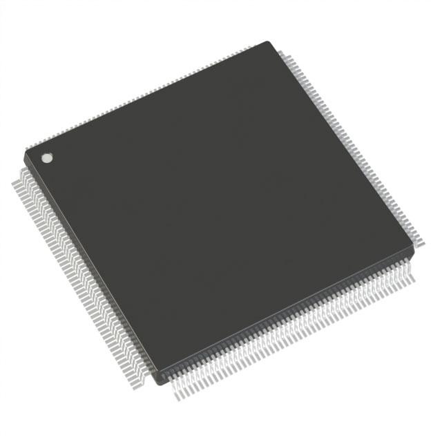
AX500-2PQG208I
AX500-2PQG208I ECAD Model
AX500-2PQG208I Attributes
| Type | Description | Select |
|---|---|---|
| Rohs Code | Yes | |
| Part Life Cycle Code | Transferred | |
| Supply Voltage-Nom | 1.5 V | |
| Number of Inputs | 336 | |
| Number of Outputs | 336 | |
| Number of Logic Cells | 8064 | |
| Number of Equivalent Gates | 500000 | |
| Number of CLBs | 5376 | |
| Combinatorial Delay of a CLB-Max | 740 ps | |
| Programmable Logic Type | FIELD PROGRAMMABLE GATE ARRAY | |
| Temperature Grade | INDUSTRIAL | |
| Package Shape | SQUARE | |
| Technology | CMOS | |
| Organization | 5376 CLBS, 500000 GATES | |
| Additional Feature | 500000 SYSTEM GATES AVAILABLE | |
| Clock Frequency-Max | 870 MHz | |
| Power Supplies | 1.5,1.5/3.3,2.5/3.3 V | |
| Supply Voltage-Max | 1.575 V | |
| Supply Voltage-Min | 1.425 V | |
| JESD-30 Code | S-PQFP-G208 | |
| Qualification Status | Not Qualified | |
| JESD-609 Code | e3 | |
| Moisture Sensitivity Level | 3 | |
| Operating Temperature-Max | 85 °C | |
| Operating Temperature-Min | -40 °C | |
| Peak Reflow Temperature (Cel) | 245 | |
| Time@Peak Reflow Temperature-Max (s) | 30 | |
| Number of Terminals | 208 | |
| Package Body Material | PLASTIC/EPOXY | |
| Package Code | FQFP | |
| Package Equivalence Code | QFP208,1.2SQ,20 | |
| Package Shape | SQUARE | |
| Package Style | FLATPACK, FINE PITCH | |
| Surface Mount | YES | |
| Terminal Finish | MATTE TIN | |
| Terminal Form | GULL WING | |
| Terminal Pitch | 500 µm | |
| Terminal Position | QUAD | |
| Width | 28 mm | |
| Length | 28 mm | |
| Seated Height-Max | 4.1 mm | |
| Ihs Manufacturer | MICROSEMI CORP | |
| Package Description | FQFP, QFP208,1.2SQ,20 | |
| Reach Compliance Code | compliant | |
| HTS Code | 8542.39.00.01 |
AX500-2PQG208I Datasheet Download
AX500-2PQG208I Overview
The AX500-2PQG208I is a chip model from the AX500 series of FPGA (Field Programmable Gate Array) devices from Xilinx. It is suitable for a wide range of applications, including embedded systems, digital signal processing, and industrial automation.
The AX500-2PQG208I is a low-power device with an operating voltage range of 1.14V to 1.26V. It has a total of 208 I/O pins, with two banks of 104 I/O pins each. The I/O pins are organized into two groups, with one group of 64 pins supporting 3.3V logic levels, and the other group of 144 pins supporting 1.8V logic levels. The device also features an integrated clock management unit (CMU) and a dual-channel DDR3 memory controller.
The AX500-2PQG208I has a total of 500K logic cells, with a total of 8 embedded hard blocks. It supports a wide range of I/O standards, including LVDS, LVCMOS, and SSTL. The device also features a low-power sleep mode, with a typical operating power consumption of 0.78W.
The AX500-2PQG208I is suitable for a wide range of applications, including automotive, industrial, consumer, and medical. It is also well-suited for use in embedded systems, digital signal processing, and industrial automation. The device is available in a 208-pin PQG208 package.
You May Also Be Interested In
4,046 In Stock
Pricing (USD)
| QTY | Unit Price | Ext Price |
|---|---|---|
| No reference price found. | ||


