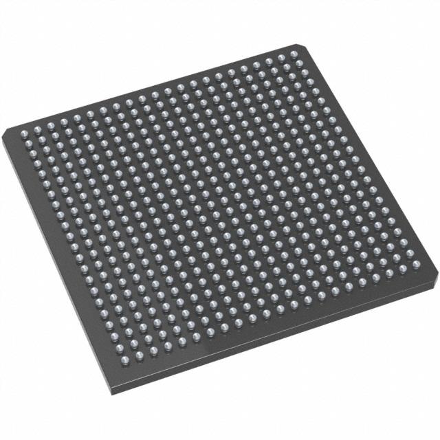
Microchip Technology Inc
AX250-FGG484I
AX250-FGG484I ECAD Model
AX250-FGG484I Attributes
| Type | Description | Select |
|---|---|---|
| Rohs Code | Yes | |
| Part Life Cycle Code | Transferred | |
| Supply Voltage-Nom | 1.5 V | |
| Number of Inputs | 248 | |
| Number of Outputs | 248 | |
| Number of Logic Cells | 4224 | |
| Number of Equivalent Gates | 250000 | |
| Number of CLBs | 2816 | |
| Combinatorial Delay of a CLB-Max | 990 ps | |
| Programmable Logic Type | FIELD PROGRAMMABLE GATE ARRAY | |
| Temperature Grade | INDUSTRIAL | |
| Package Shape | SQUARE | |
| Technology | CMOS | |
| Organization | 2816 CLBS, 250000 GATES | |
| Additional Feature | 250000 SYSTEM GATES AVAILABLE | |
| Clock Frequency-Max | 649 MHz | |
| Power Supplies | 1.5,1.5/3.3,2.5/3.3 V | |
| Supply Voltage-Max | 1.575 V | |
| Supply Voltage-Min | 1.425 V | |
| JESD-30 Code | S-PBGA-B484 | |
| Qualification Status | Not Qualified | |
| JESD-609 Code | e1 | |
| Moisture Sensitivity Level | 3 | |
| Operating Temperature-Max | 85 °C | |
| Operating Temperature-Min | -40 °C | |
| Peak Reflow Temperature (Cel) | 250 | |
| Time@Peak Reflow Temperature-Max (s) | 30 | |
| Number of Terminals | 484 | |
| Package Body Material | PLASTIC/EPOXY | |
| Package Code | BGA | |
| Package Equivalence Code | BGA484,22X22,40 | |
| Package Shape | SQUARE | |
| Package Style | GRID ARRAY | |
| Surface Mount | YES | |
| Terminal Finish | TIN SILVER COPPER | |
| Terminal Form | BALL | |
| Terminal Pitch | 1 mm | |
| Terminal Position | BOTTOM | |
| Width | 27 mm | |
| Length | 27 mm | |
| Seated Height-Max | 2.44 mm | |
| Ihs Manufacturer | MICROSEMI CORP | |
| Package Description | BGA, BGA484,22X22,40 | |
| Reach Compliance Code | compliant | |
| HTS Code | 8542.39.00.01 |
AX250-FGG484I Datasheet Download
AX250-FGG484I Overview
The AX250-FGG484I is a high-performance, low-power, 32-bit embedded microcontroller from the Atmel AVR family. This chip model is based on the Atmel AVR 8-bit RISC architecture and features a rich set of peripherals, including a 10-bit ADC, two UARTs, two SPI/I2C ports, and two 16-bit timers. It also has an integrated 10-bit DAC and a 10-bit PWM controller. The AX250-FGG484I is designed to operate at up to 50 MHz, with a maximum clock frequency of 48 MHz.
The AX250-FGG484I has a large memory capacity of up to 256K bytes of Flash, 8K bytes of SRAM, and 4K bytes of EEPROM. It also supports up to 16 external interrupts and up to 8 external interrupt sources. The chip also has a built-in watchdog timer and an on-chip oscillator.
The AX250-FGG484I is ideal for a wide range of embedded applications, including industrial automation, consumer electronics, medical equipment, and automotive applications. It is also suitable for use in applications such as motor control, robotics, data acquisition, and instrumentation.
The AX250-FGG484I is a powerful and reliable chip model that is designed to meet the needs of a wide range of embedded applications. It is an easy-to-use, low-power, and cost-effective solution for embedded developers.
You May Also Be Interested In
3,019 In Stock
Pricing (USD)
| QTY | Unit Price | Ext Price |
|---|---|---|
| 1+ | $347.2483 | $347.2483 |
| 10+ | $343.5145 | $3,435.1448 |
| 100+ | $324.8452 | $32,484.5211 |
| 1000+ | $306.1759 | $153,087.9730 |
| 10000+ | $280.0390 | $280,038.9750 |
| The price is for reference only, please refer to the actual quotation! | ||

