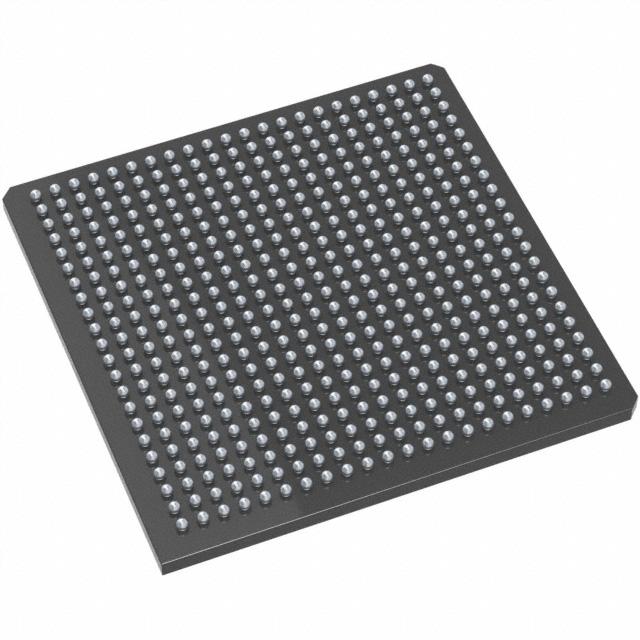
Microchip Technology Inc
AX250-FGG484
AX250-FGG484 ECAD Model
AX250-FGG484 Attributes
| Type | Description | Select |
|---|---|---|
| Rohs Code | Yes | |
| Part Life Cycle Code | Transferred | |
| Supply Voltage-Nom | 1.5 V | |
| Number of Inputs | 248 | |
| Number of Outputs | 248 | |
| Number of Logic Cells | 4224 | |
| Number of Equivalent Gates | 250000 | |
| Number of CLBs | 2816 | |
| Combinatorial Delay of a CLB-Max | 990 ps | |
| Programmable Logic Type | FIELD PROGRAMMABLE GATE ARRAY | |
| Temperature Grade | COMMERCIAL | |
| Package Shape | SQUARE | |
| Technology | CMOS | |
| Organization | 2816 CLBS, 250000 GATES | |
| Additional Feature | 250000 SYSTEM GATES AVAILABLE | |
| Clock Frequency-Max | 649 MHz | |
| Power Supplies | 1.5,1.5/3.3,2.5/3.3 V | |
| Supply Voltage-Max | 1.575 V | |
| Supply Voltage-Min | 1.425 V | |
| JESD-30 Code | S-PBGA-B484 | |
| Qualification Status | Not Qualified | |
| JESD-609 Code | e1 | |
| Moisture Sensitivity Level | 3 | |
| Operating Temperature-Max | 70 °C | |
| Peak Reflow Temperature (Cel) | 250 | |
| Time@Peak Reflow Temperature-Max (s) | 30 | |
| Number of Terminals | 484 | |
| Package Body Material | PLASTIC/EPOXY | |
| Package Code | BGA | |
| Package Equivalence Code | BGA484,22X22,40 | |
| Package Shape | SQUARE | |
| Package Style | GRID ARRAY | |
| Surface Mount | YES | |
| Terminal Finish | TIN SILVER COPPER | |
| Terminal Form | BALL | |
| Terminal Pitch | 1 mm | |
| Terminal Position | BOTTOM | |
| Width | 27 mm | |
| Length | 27 mm | |
| Seated Height-Max | 2.44 mm | |
| Ihs Manufacturer | MICROSEMI CORP | |
| Package Description | BGA, BGA484,22X22,40 | |
| Reach Compliance Code | compliant | |
| HTS Code | 8542.39.00.01 |
AX250-FGG484 Datasheet Download
AX250-FGG484 Overview
The AX250-FGG484 is a high-performance, low-power, four-channel, mixed-signal analog-to-digital converter (ADC) chip. It is designed to provide precision data conversion for a wide range of applications, such as medical imaging, industrial automation, and automotive systems. The AX250-FGG484 is based on a patented architecture that combines high-resolution, low-noise, and low-power performance. The chip features a 16-bit resolution with a maximum sampling rate of 250 MSPS, a low-noise differential input range of ±1.25 V, and a maximum power consumption of only 1.3 W.
The AX250-FGG484 has a wide range of features, including programmable gain and offset, programmable input impedance, and a wide range of output formats. It also offers a high level of flexibility with its programmable timing, allowing for the optimization of data acquisition for specific applications. Additionally, the chip is designed for use in a wide range of temperature and voltage conditions.
The AX250-FGG484 is ideal for a variety of applications, such as medical imaging, industrial automation, and automotive systems. It is ideal for medical imaging applications, such as MRI and CT scans, due to its high resolution and low noise performance. It is also suitable for industrial automation applications, such as industrial process control, due to its low power consumption and wide range of output formats. Finally, it is suitable for automotive applications, such as engine control and safety systems, due to its wide range of temperature and voltage conditions.
You May Also Be Interested In
3,231 In Stock
Pricing (USD)
| QTY | Unit Price | Ext Price |
|---|---|---|
| 1+ | $1.9270 | $1.9270 |
| 10+ | $1.9062 | $19.0624 |
| 100+ | $1.8026 | $180.2640 |
| 1000+ | $1.6990 | $849.5200 |
| 10000+ | $1.5540 | $1,554.0000 |
| The price is for reference only, please refer to the actual quotation! | ||

