
Microchip Technology Inc
AX250-FG484M
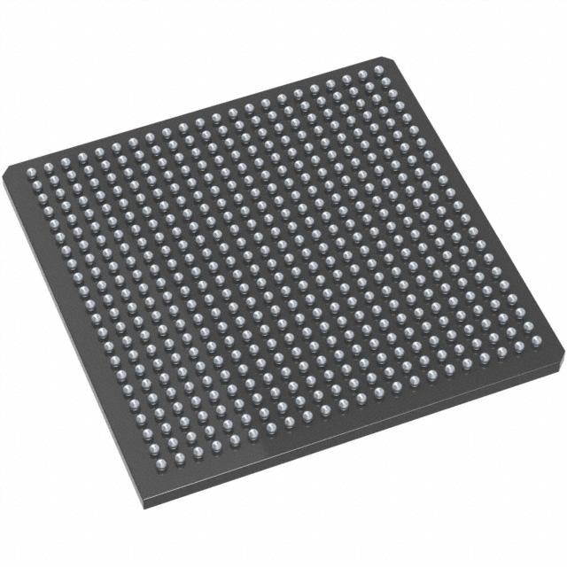
AX250-FG484M ECAD Model
AX250-FG484M Attributes
| Type | Description | Select |
|---|---|---|
| Rohs Code | No | |
| Part Life Cycle Code | Transferred | |
| Supply Voltage-Nom | 1.5 V | |
| Number of Inputs | 248 | |
| Number of Outputs | 248 | |
| Number of Logic Cells | 4224 | |
| Number of Equivalent Gates | 250000 | |
| Number of CLBs | 2816 | |
| Combinatorial Delay of a CLB-Max | 990 ps | |
| Programmable Logic Type | FIELD PROGRAMMABLE GATE ARRAY | |
| Screening Level | MIL-STD-883 Class B | |
| Temperature Grade | MILITARY | |
| Package Shape | SQUARE | |
| Technology | CMOS | |
| Organization | 2816 CLBS, 250000 GATES | |
| Additional Feature | 250000 SYSTEM GATES AVAILABLE | |
| Clock Frequency-Max | 649 MHz | |
| Power Supplies | 1.5,1.5/3.3,2.5/3.3 V | |
| Supply Voltage-Max | 1.575 V | |
| Supply Voltage-Min | 1.425 V | |
| JESD-30 Code | S-PBGA-B484 | |
| Qualification Status | Not Qualified | |
| JESD-609 Code | e0 | |
| Moisture Sensitivity Level | 3 | |
| Operating Temperature-Max | 125 °C | |
| Operating Temperature-Min | -55 °C | |
| Number of Terminals | 484 | |
| Package Body Material | PLASTIC/EPOXY | |
| Package Code | BGA | |
| Package Equivalence Code | BGA484,22X22,40 | |
| Package Shape | SQUARE | |
| Package Style | GRID ARRAY | |
| Surface Mount | YES | |
| Terminal Finish | TIN LEAD | |
| Terminal Form | BALL | |
| Terminal Pitch | 1 mm | |
| Terminal Position | BOTTOM | |
| Width | 27 mm | |
| Length | 27 mm | |
| Seated Height-Max | 2.44 mm | |
| Ihs Manufacturer | MICROSEMI CORP | |
| Package Description | BGA, BGA484,22X22,40 | |
| Reach Compliance Code | unknown | |
| ECCN Code | 3A001.A.2.C | |
| HTS Code | 8542.39.00.01 |
AX250-FG484M Datasheet Download
AX250-FG484M Overview
The AX250-FG484M is a high-performance, low-power integrated circuit developed by Xilinx. It is a Field Programmable Gate Array (FPGA) chip that can be used for a variety of applications. The chip is based on the Xilinx Virtex-4 FPGA family and is designed for high-speed signal processing, signal integrity, and system-level integration. It features a wide range of programmable logic, memory, and I/O elements to enable the design of complex systems.
The AX250-FG484M is manufactured using a low-power 0.13 micron CMOS process, and is available in a 484-pin Flip-Chip Ball Grid Array (FCBGA) package. It has a total of 250K logic elements, 2.5Mbits of RAM, and a maximum clock frequency of 250MHz. It also includes a variety of I/O options, including high-speed differential I/O, LVDS, and single-ended I/O.
The AX250-FG484M is suitable for a wide range of applications, including high-speed communication systems, system-level integration, and embedded applications. It can be used in a variety of applications such as data acquisition systems, industrial automation, medical imaging, and automotive electronics, among others. It is also suitable for use in high-performance computing applications, such as high-speed signal processing and DSP applications.
The AX250-FG484M is a powerful, low-power FPGA chip that is suitable for a wide range of applications. It features a wide range of programmable logic, memory, and I/O elements to enable the design of complex systems. It is also suitable for use in high-performance computing applications, such as high-speed signal processing and DSP applications.
You May Also Be Interested In

1,622 In Stock
Pricing (USD)
| QTY | Unit Price | Ext Price |
|---|---|---|
| 1+ | $3,748.6070 | $3,748.6070 |
| 10+ | $3,708.2994 | $37,082.9938 |
| 100+ | $3,506.7614 | $350,676.1374 |
| 1000+ | $3,305.2234 | $1,652,611.6820 |
| 10000+ | $3,023.0702 | $3,023,070.1500 |
| The price is for reference only, please refer to the actual quotation! | ||