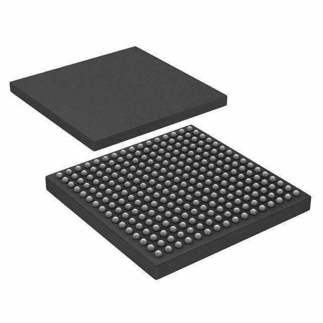
Microchip Technology Inc
AX250-FG256I
AX250-FG256I ECAD Model
AX250-FG256I Attributes
| Type | Description | Select |
|---|---|---|
| Rohs Code | No | |
| Part Life Cycle Code | Transferred | |
| Supply Voltage-Nom | 1.5 V | |
| Number of Inputs | 248 | |
| Number of Outputs | 248 | |
| Number of Logic Cells | 4224 | |
| Number of Equivalent Gates | 250000 | |
| Number of CLBs | 2816 | |
| Combinatorial Delay of a CLB-Max | 990 ps | |
| Programmable Logic Type | FIELD PROGRAMMABLE GATE ARRAY | |
| Temperature Grade | INDUSTRIAL | |
| Package Shape | SQUARE | |
| Technology | CMOS | |
| Organization | 2816 CLBS, 250000 GATES | |
| Additional Feature | 250000 SYSTEM GATES AVAILABLE | |
| Clock Frequency-Max | 649 MHz | |
| Power Supplies | 1.5,1.5/3.3,2.5/3.3 V | |
| Supply Voltage-Max | 1.575 V | |
| Supply Voltage-Min | 1.425 V | |
| JESD-30 Code | S-PBGA-B256 | |
| Qualification Status | Not Qualified | |
| JESD-609 Code | e0 | |
| Moisture Sensitivity Level | 3 | |
| Operating Temperature-Max | 85 °C | |
| Operating Temperature-Min | -40 °C | |
| Peak Reflow Temperature (Cel) | 225 | |
| Time@Peak Reflow Temperature-Max (s) | 20 | |
| Number of Terminals | 256 | |
| Package Body Material | PLASTIC/EPOXY | |
| Package Code | LBGA | |
| Package Equivalence Code | BGA256,16X16,40 | |
| Package Shape | SQUARE | |
| Package Style | GRID ARRAY, LOW PROFILE | |
| Surface Mount | YES | |
| Terminal Finish | TIN LEAD | |
| Terminal Form | BALL | |
| Terminal Pitch | 1 mm | |
| Terminal Position | BOTTOM | |
| Width | 17 mm | |
| Length | 17 mm | |
| Seated Height-Max | 1.7 mm | |
| Ihs Manufacturer | MICROSEMI CORP | |
| Package Description | LBGA, BGA256,16X16,40 | |
| Reach Compliance Code | unknown | |
| HTS Code | 8542.39.00.01 |
AX250-FG256I Datasheet Download
AX250-FG256I Overview
The AX250-FG256I is a high-performance, low-power, low-cost FPGA chip designed by Xilinx. It is a member of the Spartan-6 family of FPGAs and is suitable for a wide range of applications.
The chip features 256 logic cells, up to 32Kbits of embedded memory, up to 90 user-defined I/O pins, and a wide variety of I/O standards, including LVDS, LVCMOS, and SSTL. It also supports multiple clock sources, including an on-board oscillator and an external clock source.
The AX250-FG256I is ideal for applications such as industrial control, communications, and medical imaging. It is capable of providing high-speed data processing, low-power consumption, and flexibility for system design.
The chip has a wide variety of features, such as programmable logic, embedded memory, and I/O capabilities. It also has a high-speed transceiver, which enables it to support data rates up to 6.25Gbps.
The AX250-FG256I is a reliable and cost-effective FPGA chip that can be used in a variety of applications. It is a great choice for designers who need a highly flexible and powerful FPGA solution.
You May Also Be Interested In
5,366 In Stock
Pricing (USD)
| QTY | Unit Price | Ext Price |
|---|---|---|
| No reference price found. | ||

