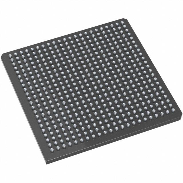
Microchip Technology Inc
AX250-1FGG484I
AX250-1FGG484I ECAD Model
AX250-1FGG484I Attributes
| Type | Description | Select |
|---|---|---|
| Rohs Code | Yes | |
| Part Life Cycle Code | Transferred | |
| Supply Voltage-Nom | 1.5 V | |
| Number of Inputs | 248 | |
| Number of Outputs | 248 | |
| Number of Logic Cells | 4224 | |
| Number of Equivalent Gates | 250000 | |
| Number of CLBs | 2816 | |
| Combinatorial Delay of a CLB-Max | 840 ps | |
| Programmable Logic Type | FIELD PROGRAMMABLE GATE ARRAY | |
| Temperature Grade | INDUSTRIAL | |
| Package Shape | SQUARE | |
| Technology | CMOS | |
| Organization | 2816 CLBS, 250000 GATES | |
| Additional Feature | 250000 SYSTEM GATES AVAILABLE | |
| Clock Frequency-Max | 763 MHz | |
| Power Supplies | 1.5,1.5/3.3,2.5/3.3 V | |
| Supply Voltage-Max | 1.575 V | |
| Supply Voltage-Min | 1.425 V | |
| JESD-30 Code | S-PBGA-B484 | |
| Qualification Status | Not Qualified | |
| JESD-609 Code | e1 | |
| Moisture Sensitivity Level | 3 | |
| Operating Temperature-Max | 85 °C | |
| Operating Temperature-Min | -40 °C | |
| Peak Reflow Temperature (Cel) | 250 | |
| Time@Peak Reflow Temperature-Max (s) | 30 | |
| Number of Terminals | 484 | |
| Package Body Material | PLASTIC/EPOXY | |
| Package Code | BGA | |
| Package Equivalence Code | BGA484,22X22,40 | |
| Package Shape | SQUARE | |
| Package Style | GRID ARRAY | |
| Surface Mount | YES | |
| Terminal Finish | TIN SILVER COPPER | |
| Terminal Form | BALL | |
| Terminal Pitch | 1 mm | |
| Terminal Position | BOTTOM | |
| Width | 27 mm | |
| Length | 27 mm | |
| Seated Height-Max | 2.44 mm | |
| Ihs Manufacturer | MICROSEMI CORP | |
| Package Description | BGA, BGA484,22X22,40 | |
| Reach Compliance Code | compliant | |
| HTS Code | 8542.39.00.01 |
AX250-1FGG484I Datasheet Download
AX250-1FGG484I Overview
The AX250-1FGG484I is an integrated circuit (IC) chip from the AX250 family of products manufactured by Analog Devices. It is a dual-channel, low-power, low-noise amplifier designed for applications such as ultrasonic imaging, communications, and medical imaging.
The chip is built on a 0.25-micron CMOS process and has a supply voltage range of 1.8V to 3.6V. It has a noise figure of 0.7 dB and can provide a gain of up to 24 dB. The chip also has a high input dynamic range of up to 92 dB and an output dynamic range of up to 72 dB. In addition, the chip has a wide bandwidth of up to 1.8 GHz and a low distortion of -72 dBc.
The AX250-1FGG484I is ideal for applications that require low power consumption, low noise, and high linearity. It can be used in ultrasound imaging systems, medical imaging systems, communications systems, and other applications that require high-performance amplifiers. It is also suitable for applications such as cellular base stations, Wi-Fi access points, and other wireless communication systems.
Overall, the AX250-1FGG484I is an excellent choice for applications that require low-noise, low-power, and high-linearity amplifiers. It has a wide bandwidth and low distortion, making it an ideal choice for a variety of applications.
You May Also Be Interested In
2,884 In Stock
Pricing (USD)
| QTY | Unit Price | Ext Price |
|---|---|---|
| 1+ | $300.5834 | $300.5834 |
| 10+ | $297.3514 | $2,973.5136 |
| 100+ | $281.1910 | $28,119.0960 |
| 1000+ | $265.0306 | $132,515.2800 |
| 10000+ | $242.4060 | $242,406.0000 |
| The price is for reference only, please refer to the actual quotation! | ||

