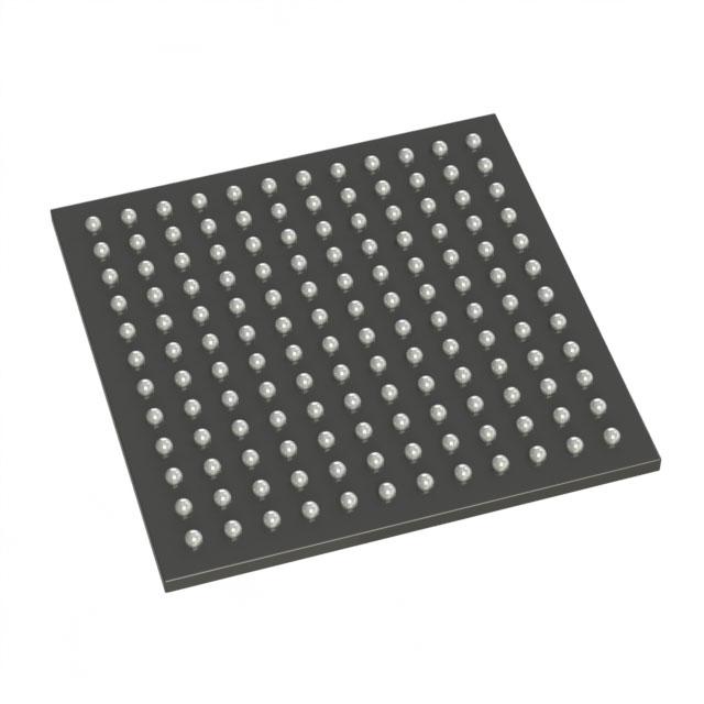
Microchip Technology Inc
APA450-FGG144I
APA450-FGG144I ECAD Model
APA450-FGG144I Attributes
| Type | Description | Select |
|---|---|---|
| Rohs Code | Yes | |
| Part Life Cycle Code | Transferred | |
| Supply Voltage-Nom | 2.5 V | |
| Number of Inputs | 100 | |
| Number of Outputs | 100 | |
| Number of Logic Cells | 12288 | |
| Number of Equivalent Gates | 450000 | |
| Programmable Logic Type | FIELD PROGRAMMABLE GATE ARRAY | |
| Temperature Grade | INDUSTRIAL | |
| Package Shape | SQUARE | |
| Technology | CMOS | |
| Organization | 450000 GATES | |
| Clock Frequency-Max | 180 MHz | |
| Power Supplies | 2.5,2.5/3.3 V | |
| Supply Voltage-Max | 2.7 V | |
| Supply Voltage-Min | 2.3 V | |
| JESD-30 Code | S-PBGA-B144 | |
| Qualification Status | Not Qualified | |
| JESD-609 Code | e1 | |
| Moisture Sensitivity Level | 3 | |
| Operating Temperature-Max | 85 °C | |
| Operating Temperature-Min | -40 °C | |
| Peak Reflow Temperature (Cel) | 260 | |
| Time@Peak Reflow Temperature-Max (s) | 30 | |
| Number of Terminals | 144 | |
| Package Body Material | PLASTIC/EPOXY | |
| Package Code | LBGA | |
| Package Equivalence Code | BGA144,12X12,40 | |
| Package Shape | SQUARE | |
| Package Style | GRID ARRAY, LOW PROFILE | |
| Surface Mount | YES | |
| Terminal Finish | Tin/Silver/Copper (Sn/Ag/Cu) | |
| Terminal Form | BALL | |
| Terminal Pitch | 1 mm | |
| Terminal Position | BOTTOM | |
| Width | 13 mm | |
| Length | 13 mm | |
| Seated Height-Max | 1.55 mm | |
| Ihs Manufacturer | MICROSEMI CORP | |
| Package Description | LBGA, BGA144,12X12,40 | |
| Reach Compliance Code | compliant | |
| HTS Code | 8542.39.00.01 |
APA450-FGG144I Datasheet Download
APA450-FGG144I Overview
The APA450-FGG144I is a low-power, high-performance Field Programmable Gate Array (FPGA) chip manufactured by Altera Corporation. It is designed for a variety of applications, such as embedded control, industrial automation, and communications. The chip features 144,000 logic elements, which provide up to 4,608 Kbits of embedded RAM and up to 1,152 Kbits of embedded ROM. It also has up to 9,600 user I/O pins, and is capable of operating at up to 400 MHz.
The APA450-FGG144I is built on a low-power, high-performance architecture, and is capable of implementing multiple clock domains to support high-speed data processing. It also features a low-power, high-performance DSP block, which provides up to 8,192 8-bit MACs per cycle. Additionally, the chip supports up to 16,384 user-defined I/O pins and up to 4,608 Kbits of embedded RAM, making it suitable for a wide range of applications.
The chip also features an on-chip power management unit, which allows for dynamic power management and efficient power management. This power management unit allows the chip to be used in a wide range of applications, such as embedded control, industrial automation, and communications. Additionally, the chip is designed to meet a variety of requirements, including high-speed data processing, low-power operation, and high-density I/O.
Overall, the APA450-FGG144I is a low-power, high-performance FPGA chip designed for a variety of applications. It features 144,000 logic elements, up to 9,600 user I/O pins, and is capable of operating at up to 400 MHz. Additionally, it supports multiple clock domains and a low-power, high-performance DSP block, making it suitable for a wide range of applications.
You May Also Be Interested In
2,182 In Stock
Pricing (USD)
| QTY | Unit Price | Ext Price |
|---|---|---|
| No reference price found. | ||

