
Microchip Technology Inc
AGLN250V5-CSG81
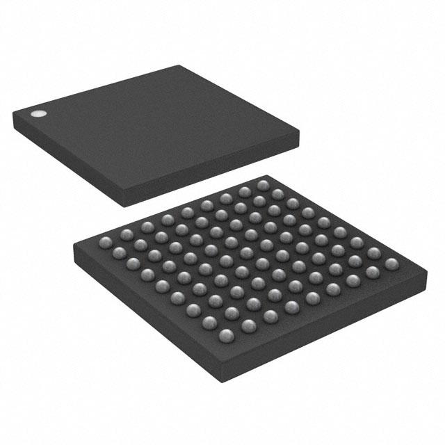
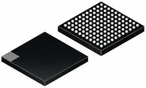
AGLN250V5-CSG81 ECAD Model
AGLN250V5-CSG81 Attributes
| Type | Description | Select |
|---|---|---|
| Rohs Code | Yes | |
| Part Life Cycle Code | Transferred | |
| Supply Voltage-Nom | 1.5 V | |
| Number of Equivalent Gates | 250000 | |
| Number of CLBs | 6144 | |
| Programmable Logic Type | FIELD PROGRAMMABLE GATE ARRAY | |
| Temperature Grade | OTHER | |
| Package Shape | SQUARE | |
| Technology | CMOS | |
| Organization | 6144 CLBS, 250000 GATES | |
| Supply Voltage-Max | 1.575 V | |
| Supply Voltage-Min | 1.425 V | |
| JESD-30 Code | S-PBGA-B81 | |
| Qualification Status | Not Qualified | |
| Moisture Sensitivity Level | 3 | |
| Operating Temperature-Max | 70 °C | |
| Operating Temperature-Min | -20 °C | |
| Peak Reflow Temperature (Cel) | 260 | |
| Time@Peak Reflow Temperature-Max (s) | 30 | |
| Number of Terminals | 81 | |
| Package Body Material | PLASTIC/EPOXY | |
| Package Code | VFBGA | |
| Package Shape | SQUARE | |
| Package Style | GRID ARRAY, VERY THIN PROFILE, FINE PITCH | |
| Surface Mount | YES | |
| Terminal Form | BALL | |
| Terminal Pitch | 500 µm | |
| Terminal Position | BOTTOM | |
| Width | 5 mm | |
| Length | 5 mm | |
| Seated Height-Max | 800 µm | |
| Ihs Manufacturer | MICROSEMI CORP | |
| Package Description | VFBGA, | |
| Reach Compliance Code | compliant | |
| HTS Code | 8542.39.00.01 |
AGLN250V5-CSG81 Datasheet Download
AGLN250V5-CSG81 Overview
The AGLN250V5-CSG81 is an advanced low-power, high-performance programmable logic device (PLD) from Altera Corporation. It is designed to provide a high-performance, cost-effective solution for applications requiring large amounts of logic and memory. The device is available in a 5x5 mm package and has a maximum operating frequency of 250 MHz.
The AGLN250V5-CSG81 includes 8-input look-up tables (LUTs), 32Kbits of RAM, and up to 4Kbits of user-defined logic (UDL). It also includes two dedicated PLLs, two clock management blocks, and two dedicated high-speed transceivers. The device supports up to 8 user-defined input/output (I/O) signals and has programmable I/O standards, including LVDS and LVCMOS. The device also features on-chip power management, allowing for low-power operation and improved system reliability.
The AGLN250V5-CSG81 is suitable for a variety of applications, including wireless communication, digital signal processing (DSP), image processing, and automotive systems. It is also ideal for use in industrial automation, medical imaging, and consumer electronics. The device is designed to be used in systems that require high-performance, low-power operation, and is compatible with Altera's Quartus II software.
Overall, the AGLN250V5-CSG81 is a high-performance, low-power programmable logic device that is suitable for a variety of applications. It has a maximum operating frequency of 250 MHz and includes 8-input LUTs, 32Kbits of RAM, and up to 4Kbits of UDL. The device is also compatible with Altera's Quartus II software and features on-chip power management for improved system reliability.
You May Also Be Interested In

5,251 In Stock
Pricing (USD)
| QTY | Unit Price | Ext Price |
|---|---|---|
| 1+ | $21.1600 | $21.1600 |
| 10+ | $20.9325 | $209.3248 |
| 100+ | $19.7948 | $1,979.4849 |
| 1000+ | $18.6572 | $9,328.6070 |
| 10000+ | $17.0645 | $17,064.5250 |
| The price is for reference only, please refer to the actual quotation! | ||