
Microchip Technology Inc
AGL250V2-VQ100
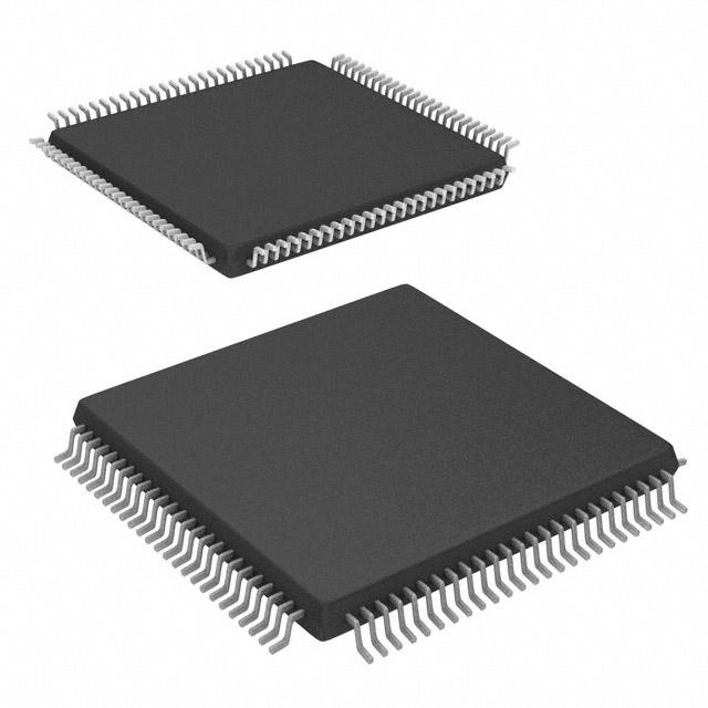
AGL250V2-VQ100 ECAD Model
AGL250V2-VQ100 Attributes
| Type | Description | Select |
|---|---|---|
| Rohs Code | No | |
| Part Life Cycle Code | Transferred | |
| Supply Voltage-Nom | 1.2 V | |
| Number of Equivalent Gates | 250000 | |
| Number of CLBs | 6144 | |
| Programmable Logic Type | FIELD PROGRAMMABLE GATE ARRAY | |
| Temperature Grade | OTHER | |
| Package Shape | SQUARE | |
| Technology | CMOS | |
| Organization | 6144 CLBS, 250000 GATES | |
| Clock Frequency-Max | 108 MHz | |
| Supply Voltage-Max | 1.575 V | |
| Supply Voltage-Min | 1.14 V | |
| JESD-30 Code | S-PQFP-G100 | |
| Qualification Status | Not Qualified | |
| JESD-609 Code | e0 | |
| Moisture Sensitivity Level | 3 | |
| Operating Temperature-Max | 85 °C | |
| Number of Terminals | 100 | |
| Package Body Material | PLASTIC/EPOXY | |
| Package Code | TFQFP | |
| Package Shape | SQUARE | |
| Package Style | FLATPACK, THIN PROFILE, FINE PITCH | |
| Surface Mount | YES | |
| Terminal Finish | TIN LEAD | |
| Terminal Form | GULL WING | |
| Terminal Pitch | 500 µm | |
| Terminal Position | QUAD | |
| Width | 14 mm | |
| Length | 14 mm | |
| Seated Height-Max | 1.2 mm | |
| Ihs Manufacturer | MICROSEMI CORP | |
| Package Description | TFQFP, | |
| Reach Compliance Code | unknown | |
| HTS Code | 8542.39.00.01 |
AGL250V2-VQ100 Datasheet Download
AGL250V2-VQ100 Overview
The Microchip Technology model AGL250V2-VQ100 is a field-programmable gate array (FPGA) device that provides high-performance capability for embedded system designers. The device features a reconfigurable logic array, configurable arithmetic logic blocks, DDR2/DDR3 memory controllers, and high-speed serdes transceivers. The FPGA has a VQ100 package, consisting of 100 pins and a large number of gates to provide more I/Os for high-speed data communication.
The AGL250V2-VQ100 FPGA device is suitable for various applications, including communication systems, video processing, high-performance computing, and industrial control systems. It can serve as an alternative to ASICs or custom-designed system-on-chips (SoCs) since it provides a high degree of flexibility by allowing designers to reprogram the logic during runtime. Additionally, the FPGA supports a range of interfaces such as Gigabit Ethernet, HDMI, PCIe, and High-Speed USB to suit a variety of communication requirements.
The device comes with a design suite called Libero® which includes a Graphical User Interface (GUI) with built-in software modules and an embedded software design flow, making it easier for designers to build, verify, and implement their designs. The software suite also includes debugging tools and system integration facilities to ease the integration of the AGL250V2-VQ100 FPGA device in the final design.
In conclusion, the AGL250V2-VQ100 FPGA is a versatile and high-performance device that provides significant advantages for embedded systems designers in a wide range of industries, from communication and computing to video processing and industrial control systems. Its flexibility, large number of I/Os, and high processing speed make it an ideal solution for demanding applications.
You May Also Be Interested In

5,987 In Stock
Pricing (USD)
| QTY | Unit Price | Ext Price |
|---|---|---|
| 1+ | $19.7309 | $19.7309 |
| 10+ | $19.5187 | $195.1872 |
| 100+ | $18.4579 | $1,845.7920 |
| 1000+ | $17.3971 | $8,698.5600 |
| 10000+ | $15.9120 | $15,912.0000 |
| The price is for reference only, please refer to the actual quotation! | ||