
Microchip Technology Inc
A54SX72A-2FGG484I
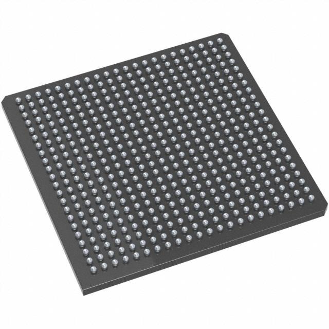
A54SX72A-2FGG484I ECAD Model
A54SX72A-2FGG484I Attributes
| Type | Description | Select |
|---|---|---|
| Rohs Code | Yes | |
| Part Life Cycle Code | Transferred | |
| Supply Voltage-Nom | 2.5 V | |
| Number of Inputs | 360 | |
| Number of Outputs | 360 | |
| Number of Logic Cells | 6036 | |
| Number of Equivalent Gates | 108000 | |
| Number of CLBs | 6036 | |
| Combinatorial Delay of a CLB-Max | 1.1 ns | |
| Programmable Logic Type | FIELD PROGRAMMABLE GATE ARRAY | |
| Temperature Grade | INDUSTRIAL | |
| Package Shape | SQUARE | |
| Technology | CMOS | |
| Organization | 6036 CLBS, 108000 GATES | |
| Additional Feature | 72000 TYPICAL GATES AVAILABLE | |
| Clock Frequency-Max | 294 MHz | |
| Power Supplies | 2.5,3.3/5 V | |
| Supply Voltage-Max | 2.75 V | |
| Supply Voltage-Min | 2.25 V | |
| JESD-30 Code | S-PBGA-B484 | |
| Qualification Status | Not Qualified | |
| JESD-609 Code | e1 | |
| Moisture Sensitivity Level | 3 | |
| Operating Temperature-Max | 85 °C | |
| Operating Temperature-Min | -40 °C | |
| Peak Reflow Temperature (Cel) | 250 | |
| Time@Peak Reflow Temperature-Max (s) | 30 | |
| Number of Terminals | 484 | |
| Package Body Material | PLASTIC/EPOXY | |
| Package Code | BGA | |
| Package Equivalence Code | BGA484,26X26,40 | |
| Package Shape | SQUARE | |
| Package Style | GRID ARRAY | |
| Surface Mount | YES | |
| Terminal Finish | TIN SILVER COPPER | |
| Terminal Form | BALL | |
| Terminal Pitch | 1 mm | |
| Terminal Position | BOTTOM | |
| Width | 27 mm | |
| Length | 27 mm | |
| Seated Height-Max | 2.44 mm | |
| Ihs Manufacturer | MICROSEMI CORP | |
| Package Description | BGA, BGA484,26X26,40 | |
| Reach Compliance Code | compliant | |
| HTS Code | 8542.39.00.01 |
A54SX72A-2FGG484I Datasheet Download
A54SX72A-2FGG484I Overview
The A54SX72A-2FGG484I is a Field Programmable Gate Array (FPGA) chip manufactured by Xilinx. It is a member of the Spartan-6 family of FPGAs, and is designed for high performance and low power applications. The chip has an area of 484-pin BGA package, and is capable of delivering up to 72K logic cells, 576Kb of Block RAM, and up to 454 18x18 multipliers. It is also equipped with four 6.25Gbps transceivers, and has a maximum power consumption of 8.5W.
The A54SX72A-2FGG484I is suitable for a wide range of applications, including communications, data processing, video processing, automotive, industrial, and medical. It is capable of providing high performance and low power consumption, making it suitable for applications that require high throughput and low power. It is also suitable for applications that require high speed transceivers, such as 10G Ethernet and PCIe.
The chip is also equipped with advanced features such as low power, clock management, and advanced I/O. It also supports a variety of industry-standard interfaces, such as JTAG, Ethernet, USB, and UART. Furthermore, it is also capable of supporting various development tools, such as Xilinx Vivado Design Suite, ISE Design Suite, and SDK.
In conclusion, the A54SX72A-2FGG484I is a powerful and versatile FPGA chip, suitable for a wide range of applications. With its high performance, low power consumption, and advanced features, it is an ideal choice for applications that require high throughput and low power consumption.
You May Also Be Interested In

2,133 In Stock
Pricing (USD)
| QTY | Unit Price | Ext Price |
|---|---|---|
| 1+ | $2,316.5313 | $2,316.5313 |
| 10+ | $2,291.6224 | $22,916.2239 |
| 100+ | $2,167.0777 | $216,707.7693 |
| 1000+ | $2,042.5330 | $1,021,266.4990 |
| 10000+ | $1,868.1704 | $1,868,170.4250 |
| The price is for reference only, please refer to the actual quotation! | ||