
Microchip Technology Inc
A54SX72A-2FG484
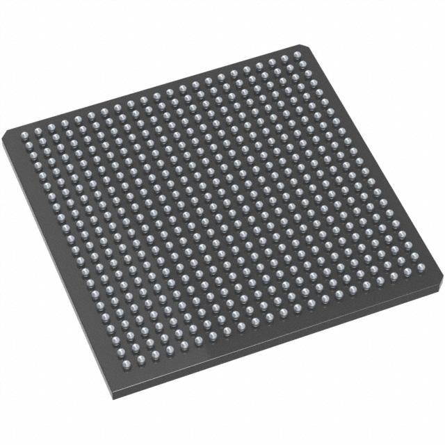
A54SX72A-2FG484 ECAD Model
A54SX72A-2FG484 Attributes
| Type | Description | Select |
|---|---|---|
| Rohs Code | No | |
| Part Life Cycle Code | Transferred | |
| Supply Voltage-Nom | 2.5 V | |
| Number of Inputs | 360 | |
| Number of Outputs | 360 | |
| Number of Logic Cells | 6036 | |
| Number of Equivalent Gates | 108000 | |
| Number of CLBs | 6036 | |
| Combinatorial Delay of a CLB-Max | 1.1 ns | |
| Programmable Logic Type | FIELD PROGRAMMABLE GATE ARRAY | |
| Temperature Grade | COMMERCIAL | |
| Package Shape | SQUARE | |
| Technology | CMOS | |
| Organization | 6036 CLBS, 108000 GATES | |
| Additional Feature | 72000 TYPICAL GATES AVAILABLE | |
| Clock Frequency-Max | 294 MHz | |
| Power Supplies | 2.5,3.3/5 V | |
| Supply Voltage-Max | 2.75 V | |
| Supply Voltage-Min | 2.25 V | |
| JESD-30 Code | S-PBGA-B484 | |
| Qualification Status | Not Qualified | |
| JESD-609 Code | e0 | |
| Moisture Sensitivity Level | 3 | |
| Operating Temperature-Max | 70 °C | |
| Number of Terminals | 484 | |
| Package Body Material | PLASTIC/EPOXY | |
| Package Code | BGA | |
| Package Equivalence Code | BGA484,26X26,40 | |
| Package Shape | SQUARE | |
| Package Style | GRID ARRAY | |
| Surface Mount | YES | |
| Terminal Finish | TIN LEAD | |
| Terminal Form | BALL | |
| Terminal Pitch | 1 mm | |
| Terminal Position | BOTTOM | |
| Width | 27 mm | |
| Length | 27 mm | |
| Seated Height-Max | 2.44 mm | |
| Ihs Manufacturer | MICROSEMI CORP | |
| Package Description | BGA, BGA484,26X26,40 | |
| Reach Compliance Code | unknown | |
| HTS Code | 8542.39.00.01 |
A54SX72A-2FG484 Datasheet Download
A54SX72A-2FG484 Overview
The A54SX72A-2FG484 is an FPGA chip from Xilinx that is designed for high-performance, high-density applications. It is a member of the Spartan-6 family and is based on the Xilinx SX architecture. This chip offers an array of features and benefits, including low power consumption, high performance, and a large number of I/O pins.
This FPGA chip is ideal for applications that require a high level of integration and performance in a small form factor. It is suitable for applications such as high-speed networking, telecom, and industrial automation. It can also be used in embedded systems and multimedia applications.
The A54SX72A-2FG484 has a total of 72,000 logic cells, with up to 484 I/O pins. It has a maximum clock frequency of 250 MHz, and a power consumption of up to 6.4 W. It also has an on-chip memory of up to 4 MB of RAM, and up to 4 MB of ROM.
The A54SX72A-2FG484 is also equipped with a variety of features, such as a programmable interconnect structure, clock management, and power management. It also has support for Xilinx’s Vivado Design Suite, which allows users to quickly and easily develop and debug their designs.
In conclusion, the A54SX72A-2FG484 is an FPGA chip from Xilinx that is ideal for applications that require a high level of integration and performance in a small form factor. It has a variety of features and benefits, and is suitable for a wide range of applications, including high-speed networking, telecom, and industrial automation.
You May Also Be Interested In


4,957 In Stock
Pricing (USD)
| QTY | Unit Price | Ext Price |
|---|---|---|
| 1+ | $532.8677 | $532.8677 |
| 10+ | $527.1379 | $5,271.3792 |
| 100+ | $498.4891 | $49,848.9120 |
| 1000+ | $469.8403 | $234,920.1600 |
| 10000+ | $429.7320 | $429,732.0000 |
| The price is for reference only, please refer to the actual quotation! | ||