
Microchip Technology Inc
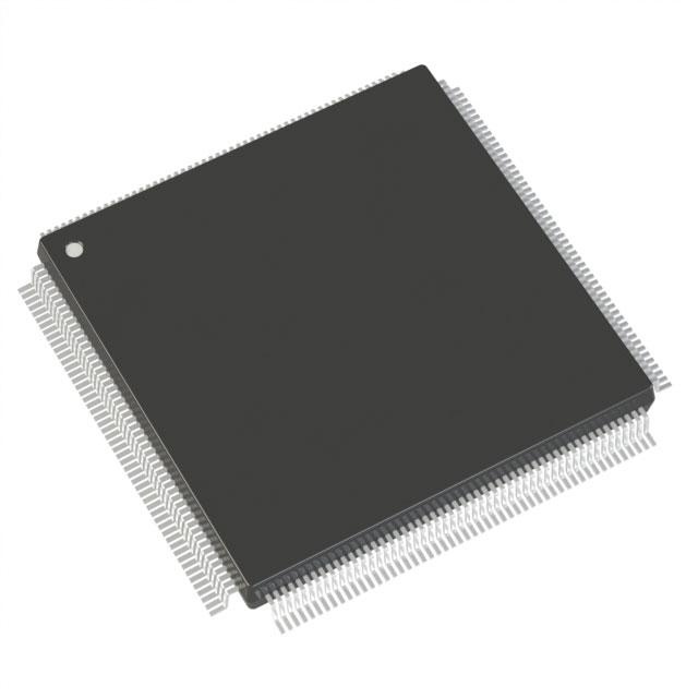
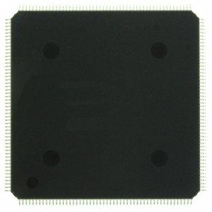
A54SX32A-2PQG208
A54SX32A-2PQG208 ECAD Model
A54SX32A-2PQG208 Attributes
| Type | Description | Select |
|---|---|---|
| Rohs Code | Yes | |
| Part Life Cycle Code | Transferred | |
| Supply Voltage-Nom | 2.5 V | |
| Number of Inputs | 174 | |
| Number of Outputs | 174 | |
| Number of Logic Cells | 2880 | |
| Number of Equivalent Gates | 48000 | |
| Number of CLBs | 2880 | |
| Combinatorial Delay of a CLB-Max | 900 ps | |
| Programmable Logic Type | FIELD PROGRAMMABLE GATE ARRAY | |
| Temperature Grade | COMMERCIAL | |
| Package Shape | SQUARE | |
| Technology | CMOS | |
| Organization | 2880 CLBS, 48000 GATES | |
| Additional Feature | 32000 TYPICAL GATES AVAILABLE | |
| Clock Frequency-Max | 313 MHz | |
| Power Supplies | 2.5,3.3/5 V | |
| Supply Voltage-Max | 2.75 V | |
| Supply Voltage-Min | 2.25 V | |
| JESD-30 Code | S-PQFP-G208 | |
| Qualification Status | Not Qualified | |
| JESD-609 Code | e3 | |
| Moisture Sensitivity Level | 3 | |
| Operating Temperature-Max | 70 °C | |
| Peak Reflow Temperature (Cel) | 245 | |
| Time@Peak Reflow Temperature-Max (s) | 30 | |
| Number of Terminals | 208 | |
| Package Body Material | PLASTIC/EPOXY | |
| Package Code | FQFP | |
| Package Equivalence Code | QFP208,1.2SQ,20 | |
| Package Shape | SQUARE | |
| Package Style | FLATPACK, FINE PITCH | |
| Surface Mount | YES | |
| Terminal Finish | MATTE TIN | |
| Terminal Form | GULL WING | |
| Terminal Pitch | 500 µm | |
| Terminal Position | QUAD | |
| Width | 28 mm | |
| Length | 28 mm | |
| Seated Height-Max | 4.1 mm | |
| Ihs Manufacturer | MICROSEMI CORP | |
| Package Description | FQFP, QFP208,1.2SQ,20 | |
| Reach Compliance Code | compliant | |
| HTS Code | 8542.39.00.01 |
A54SX32A-2PQG208 Datasheet Download
A54SX32A-2PQG208 Overview
The A54SX32A-2PQG208 is a Field Programmable Gate Array (FPGA) chip from the Xilinx Spartan-6 family. It is a high-performance, low-power FPGA with a large capacity of up to 32 million system gates. It has a total of 616 user I/O pins, including 208 differential I/O pairs. It also has 32 dedicated high-speed serial transceivers, as well as two dedicated clock management tiles. The A54SX32A-2PQG208 has an internal block RAM of up to 10.5 Mbits and a distributed RAM of up to 6.5 Mbits. It also has an internal clock management system with up to 8 PLLs and a maximum clock frequency of up to 300 MHz.
The A54SX32A-2PQG208 is suitable for a wide range of applications, such as video and image processing, high-speed communication systems, and embedded systems. It features low power consumption, high performance, and low cost, making it an ideal solution for a variety of applications. It also supports a variety of development tools, such as the Xilinx ISE Design Suite and the Xilinx Vivado Design Suite.
In summary, the A54SX32A-2PQG208 is a high-performance, low-power FPGA with a large capacity of up to 32 million system gates. It has 616 user I/O pins, 32 high-speed serial transceivers, and two dedicated clock management tiles. It is suitable for a wide range of applications, such as video and image processing, high-speed communication systems, and embedded systems. It also supports a variety of development tools, making it an ideal solution for a variety of applications.
You May Also Be Interested In

2,535 In Stock
Pricing (USD)
| QTY | Unit Price | Ext Price |
|---|---|---|
| 1+ | $229.8811 | $229.8811 |
| 10+ | $227.4093 | $2,274.0928 |
| 100+ | $215.0501 | $21,505.0080 |
| 1000+ | $202.6909 | $101,345.4400 |
| 10000+ | $185.3880 | $185,388.0000 |
| The price is for reference only, please refer to the actual quotation! | ||